Growth method of large-sized silicon carbide polycrystalline ceramic adjustable in electrical resistivity

A technology of polycrystalline ceramics and growth methods, applied in the directions of polycrystalline material growth, single crystal growth, single crystal growth, etc. The high cost of silicon production can achieve the effect of avoiding polycrystalline cracking, good density, and improving quality and yield

Active Publication Date: 2017-09-22
安徽微芯长江半导体材料有限公司
View PDF14 Cites 5 Cited by
  • Summary
  • Abstract
  • Description
  • Claims
  • Application Information

AI Technical Summary

Problems solved by technology

[0003] At present, the density, purity and thermal conductivity of traditional silicon carbide ceramics limit its wider application. Although silicon carbide single crystal has excellent performance and relatively mature preparation, it is expensive, and it is still difficult to be widely used in general. field
SiC single crystal thermal conductivity and other properties are better than SiC ceramics, but the production cost of high-quality single crystal silicon carbide is high and the process is complicated, which greatly limits the application of single crystal silicon carbide
In contrast, the preparation cost of polycrystalline silicon carbide ceramics is low and the process is relatively simple, but its density, purity and resistivity are difficult to meet the existing needs

Method used


Image

  • Growth method of large-sized silicon carbide polycrystalline ceramic adjustable in electrical resistivity
  • Growth method of large-sized silicon carbide polycrystalline ceramic adjustable in electrical resistivity
  • Growth method of large-sized silicon carbide polycrystalline ceramic adjustable in electrical resistivity

Examples


Embodiment 1

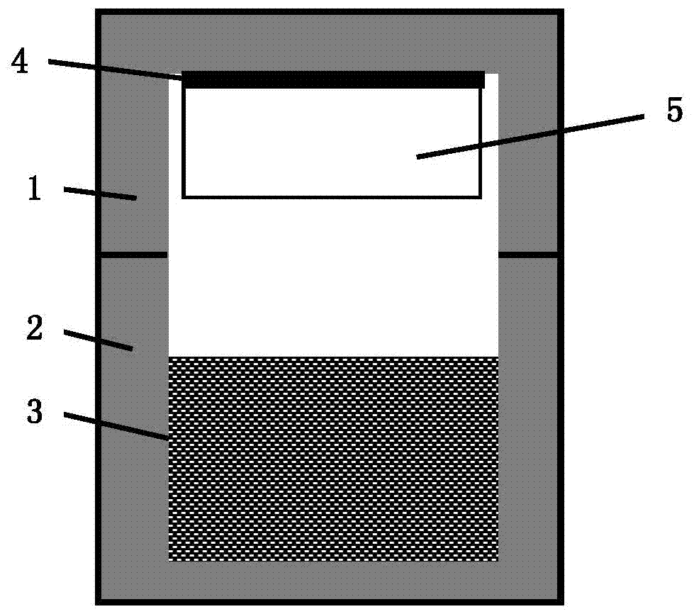
[0042] First, the graphite cover (graphite crucible top cover) coated with a carbon film layer on the top, and the graphite crucible with silicon carbide raw material (purity 99.9%) in the bottom material area are placed in the insulating carbon felt, and then put into the crystal growth furnace chamber ( The silicon carbide raw material is placed in the high temperature zone of the graphite crucible body, and the top cover of the graphite crucible with the carbon film coated on the inner surface of the growth is placed in the low temperature zone. The temperature gradient from the top cover of the graphite crucible to the bottom of the graphite crucible body is 2°C / cm. ), vacuum to 1.0×10 -2 Below Pa, fill with argon until the growth pressure is 20 Torr, and at the same time, the nitrogen flow rate is 1 sccm during the growth process, start to heat up to the growth temperature of 2080°C, after 100 hours of growth, cool down to room temperature, and open the furnace to obtain c...

Embodiment 2

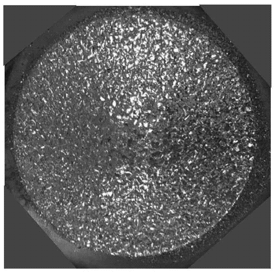
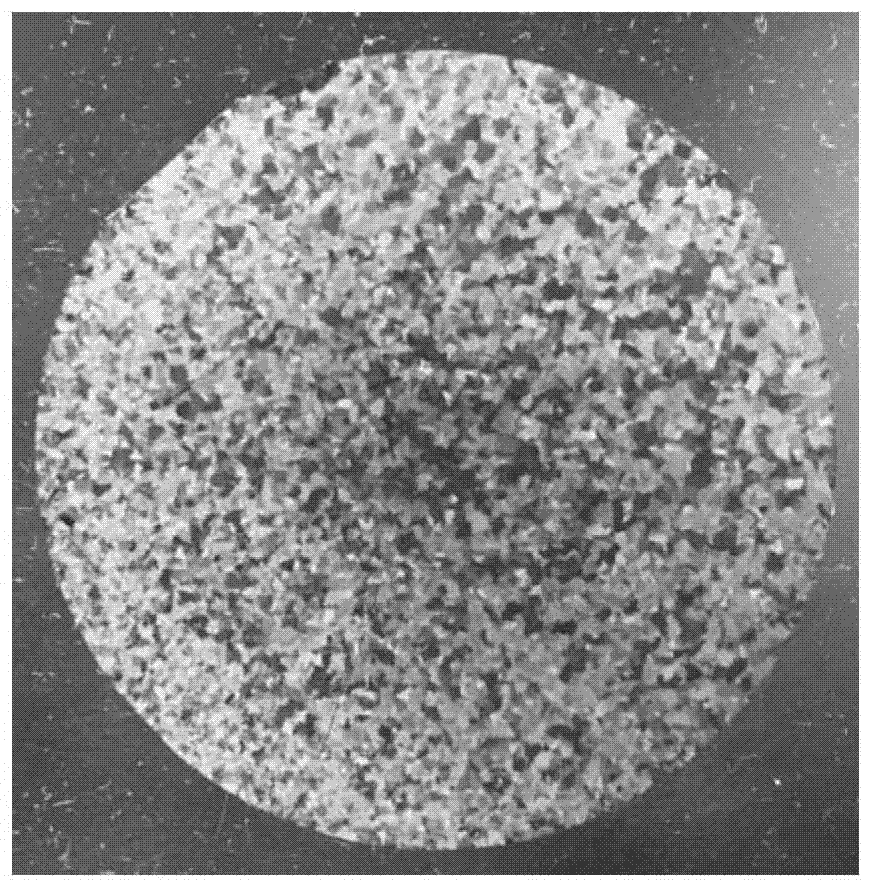
[0044] First, the graphite cover coated with a carbon film layer on the top, and the graphite crucible with silicon carbide raw material (99.9% purity) in the bottom material area are placed in the thermal insulation carbon felt, and then put into the crystal growth furnace chamber (the silicon carbide raw material is placed in In the high-temperature zone of the graphite crucible body, place the top cover of the graphite crucible coated with carbon film on the inner surface of the growth in the low-temperature zone. ×10 -2 Below Pa, fill with argon gas to a growth pressure of 10 Torr, start to heat up to a growth temperature of 2120°C, and after 100 hours of growth, cool down to room temperature with a program, and open the furnace to obtain a silicon carbide polycrystalline ceramic material with a thickness of 20 mm on a graphite cover (such as Figure 4 shown), and finally obtain silicon carbide polycrystalline ceramic sheets by mechanical processing (such as Figure 5 sho...

Embodiment 3

[0046] First, the graphite cover coated with a carbon film layer on the upper part and the graphite crucible with silicon carbide raw material (purity 99.99%) in the bottom material area are placed in the thermal insulation carbon felt, and then put into the crystal growth furnace chamber (the silicon carbide raw material is placed in In the high-temperature zone of the graphite crucible body, place the top cover of the graphite crucible coated with carbon film on the inner surface of the growth in the low-temperature zone. ×10 -2 Below Pa, fill with argon gas to a growth pressure of 10Torr, start to heat up to a growth temperature of 2120°C, after 100 hours of growth, program cooling to room temperature, open the furnace to obtain a silicon carbide polycrystalline ceramic material with a thickness of 20mm on the graphite cover, and finally through the mechanical process. Processed silicon carbide polycrystalline ceramic sheet (thickness 1mm, diameter 125mm), the measured resi...


PUM

PropertyMeasurementUnit
thicknessaaaaaaaaaa
electrical resistivityaaaaaaaaaa

Abstract

The invention relates to a growth method of a large-sized silicon carbide polycrystalline ceramic adjustable in electrical resistivity. A silicon carbide raw material is contained by adopting a graphite crucible, the graphite crucible is composed of a graphite crucible top cover and a graphite crucible body, the inner surface of the graphite crucible is provided with a carbon film layer, the silicon carbide raw material is put in the graphite crucible body, the graphite crucible top cover is put on, the graphite crucible body is put in a growth furnace, the bottom and/or the lower portion of the graphite crucible body is located in a heating zone to make the temperature at the bottom of the graphite crucible body higher than that of the graphite crucible top cover, and a silicon carbide polycrystalline ceramic material grows on the surface of the carbon film layer by adopting a physical gaseous phase transmission method or a high-temperature chemical vapor deposition method. The growth method is simple, and the silicon carbide polycrystalline ceramic is more excellent in performance, better in uniformity, better in compactness, higher in purity and better in thermal conductivity compared with a traditional silicon carbide ceramic.

Description

technical field [0001] The invention belongs to the field of silicon carbide materials, in particular to a method for growing silicon carbide polycrystalline ceramics based on a physical vapor transport method. Background technique [0002] Silicon carbide (SiC) materials mainly include two categories: single crystal and ceramics. Silicon carbide single crystal has the advantages of large band gap, high thermal conductivity, high electron saturation drift rate, high critical breakdown electric field, low dielectric constant, and good chemical stability. Irradiation semiconductor devices, ultraviolet detectors and short-wave light-emitting diodes have broad application prospects, and devices made of them can be used in high-temperature environments above 600 °C. Silicon carbide ceramics have the characteristics of high temperature strength, strong oxidation resistance, good wear resistance, good thermal stability, small thermal expansion coefficient, high thermal conductivit...

Claims


Application Information

Patent Timeline
Patent Type & Authority Applications(China)
IPC IPC(8): C30B29/36C30B28/12C30B28/14
CPCC30B28/12C30B28/14C30B29/36
Inventor 高攀忻隽陈辉刘学超郑燕青施尔畏
Owner 安徽微芯长江半导体材料有限公司
Why Eureka
Try Eureka