Method of preparing high-performance diamond semiconductor based on low-cost single crystal diamond

A single-crystal diamond and low-cost single-crystal technology, applied in semiconductor/solid-state device manufacturing, electrical components, circuits, etc., can solve the problems of reduced electrical conductivity, adverse effects of carrier transport properties, roughness, etc., to reduce defect density , Reduce technical difficulty, improve the effect of crystallization quality

Active Publication Date: 2017-10-20
UNIV OF SCI & TECH BEIJING
View PDF3 Cites 17 Cited by
  • Summary
  • Abstract
  • Description
  • Claims
  • Application Information

AI Technical Summary

Problems solved by technology

However, after the diamond surface is mechanically polished, damage layers are often produced on the surface and subsurface of the diamond substrate, resulting in epitaxially grown diamonds inheriting defects such as dislocations in the substrate, thereby affecting the carrier transport of the hydrogen-terminated surface conductive channels. adverse effects of the nature
In addition, the pure hydrogen plasma treatment will also roughen the surface of the diamond material due to etching and reduce the conductivity.

Method used


Image

  • Method of preparing high-performance diamond semiconductor based on low-cost single crystal diamond
  • Method of preparing high-performance diamond semiconductor based on low-cost single crystal diamond

Examples


Embodiment 1

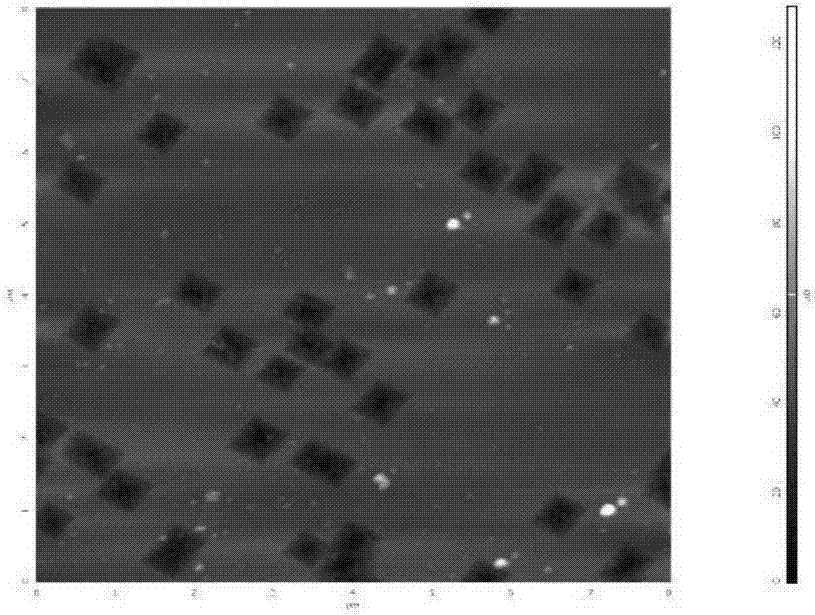
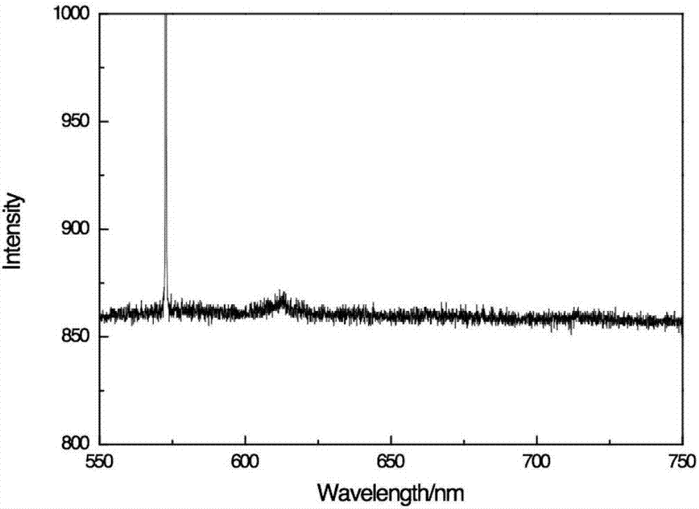
[0040] Using a high temperature and high pressure (100) oriented type Ib single crystal diamond with a side length of 4.3mm and a thickness of 0.8mm as the substrate, the single crystal diamond substrate was cleaned ultrasonically with acetone and alcohol in sequence. The ultrasonic power was 300W. 30min, blow dry. Carry out pickling and passivation treatment on the cleaned diamond substrate, place the diamond substrate in a solution with a sulfuric acid: nitric acid concentration of 5:1, and boil for 30 minutes. The diamond substrate was ultrasonically cleaned with deionized water for 2 times, with an ultrasonic power of 300 W, for 30 min each time, and then dried. The surface-passivated single-crystal diamond substrate was placed in a microwave chemical vapor deposition device, and the surface of the single-crystal diamond substrate was activated by microwave hydrogen plasma at an activation temperature of 800°C and an activation time of 5 minutes. After surface activation ...

Embodiment 2

[0042] Using a high temperature and high pressure (100) oriented type Ib single crystal diamond with a side length of 3.8mm and a thickness of 0.85mm as the substrate, the single crystal diamond substrate was cleaned ultrasonically with acetone and alcohol in sequence. The ultrasonic power was 240W. 30min, blow dry. Carry out pickling and passivation treatment on the cleaned diamond substrate, place the diamond substrate in a solution with a sulfuric acid: nitric acid concentration of 5:1, and boil for 40 minutes. The diamond substrate was ultrasonically cleaned with deionized water for 2 times, with an ultrasonic power of 240W, for 30min each time, and then dried. The surface-passivated single-crystal diamond substrate was placed in a microwave chemical vapor deposition device, and the surface of the single-crystal diamond substrate was activated by microwave hydrogen plasma at an activation temperature of 750°C and an activation time of 10 minutes. After surface activation ...

Embodiment 3

[0044] With the high temperature and high pressure (100) orientation type Ib single crystal diamond with a side length of 8 mm and a thickness of 1 mm as the substrate, the single crystal diamond substrate is cleaned ultrasonically with acetone and alcohol in sequence. The ultrasonic power is 300 W, and each cleaning is 30 minutes. blow dry. Carry out pickling and passivation treatment on the cleaned diamond substrate, place the diamond substrate in a solution with a sulfuric acid: nitric acid concentration of 5:1, and boil for 50 minutes. The diamond substrate was ultrasonically cleaned with deionized water for 2 times, with an ultrasonic power of 300 W, for 30 min each time, and then dried. The surface-passivated single-crystal diamond substrate was placed in a microwave chemical vapor deposition device, and the surface of the single-crystal diamond substrate was activated by microwave hydrogen plasma at an activation temperature of 850°C and an activation time of 3 minutes....


PUM

PropertyMeasurementUnit
surface roughnessaaaaaaaaaa
thicknessaaaaaaaaaa

Abstract

The invention discloses a method for preparing a high-performance diamond semiconductor based on low-cost single crystal diamond, and belongs to the technical field of novel semiconductor preparation. The process steps include a, a commercially available cheap high temperature and pressure Ib-type single crystal diamond substrate is subjected to acid pickling to remove surface inclusions and form a passivated oxygen termination surface; b, the activated diamond surface is subjected to short time treatment by microwave hydrogen plasmas to expose a fresh C-C dangling bond; c, a high-quality single crystal diamond thin film is epitaxially grown on the fresh diamond surface by microwave plasma chemical vapor deposition to achieve the diamond thin film epitaxy with low dislocation density and impurity content mainly through the introduction of oxygen atoms with a self-healing function; and d, a carbon source and a oxygen source are turned off, the epitaxially grown diamond surface is treated by the microwave hydrogen plasmas to obtain a high hydrogen termination density, and the treated diamond surface is cooled to room temperature under a hydrogen atmosphere to obtain a diamond semiconductor with high conductivity. According to the invention, the process flow is simplified, the technical difficulty and the production cost are reduced, and the production cycle is shortened.

Description

Technical field: [0001] The invention belongs to the technical field of novel semiconductor preparation; in particular, it provides a simple method for preparing a high-performance diamond semiconductor by using a low-cost high-temperature and high-pressure Ib-type single crystal diamond substrate, which is characterized in that the low-cost high-temperature and high-pressure diamond substrate is introduced Oxygen atoms with self-healing function realize the epitaxial growth of high-quality diamond thin layers, and realize the preparation of high-performance diamond semiconductors through activation modification in hydrogen plasma. Background technique: [0002] Due to its wide bandgap (5.5eV), high carrier mobility (especially hole mobility is much higher than single crystal Si and GaAs), high thermal conductivity (2200W / mK), high Johnson index and Keyse Indicators (both ten times higher than Si and GaAs), etc., have become the best material choice for applications in the f...

Claims


Application Information

Patent Timeline
Patent Type & Authority Applications(China)
IPC IPC(8): H01L21/02
Inventor 刘金龙李成明林亮珍郑宇亭赵云闫雄伯陈良贤魏俊俊黑立富张建军
Owner UNIV OF SCI & TECH BEIJING
Why Eureka
Try Eureka