Selective emitter junction and tunneling oxide efficient N-type battery preparation method

A technology of tunnel oxidation and emitter junction, applied in photovoltaic power generation, circuits, electrical components, etc., can solve the problems of high equipment cost, little improvement in electrical performance, poor repeatability, etc., to improve the composite speed and achieve large-scale Mass production, reducing the effect of frontal compounding

Inactive Publication Date: 2017-12-15
SHANGHAI SHENZHOU NEW ENERGY DEV
View PDF5 Cites 23 Cited by
  • Summary
  • Abstract
  • Description
  • Claims
  • Application Information

AI Technical Summary

Problems solved by technology

Selective emitter junction solar cells effectively solve this pair of contradictions, but the cost of existing equipment is high, or the repeatability is poor, and the cell preparation methods are not very ideal
[0004] Chinese patent CN102544198A discloses a method for preparing a selective emission crystalline silicon solar cell, including single-step high-concentration doping diffusion, and then printing anti-corrosion paste on the electrode area by printing process, and chemically etching the non-electrode area to achieve light doping The emitter junction, and then remove the anti-corrosion barrier layer, and finally use the conventional solar energy preparation method to make the selective emission crystalline silicon solar cell, but this patent application still uses the back point contact of the N-type crystalline silicon cell, so the electrical performance is not great. improvement

Method used


Image

  • Selective emitter junction and tunneling oxide efficient N-type battery preparation method

Examples


Embodiment 1

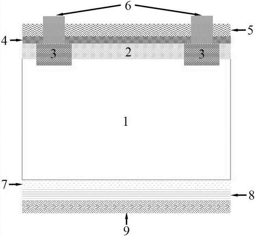
[0034] Selective emitter junction and tunnel oxidation high-efficiency N-type battery preparation method, the method uses the following steps, the structure of the prepared crystalline silicon battery is as follows figure 1 Shown:

[0035] (1) In alkaline solution, remove the damaged layer of silicon chip 1, and carry out texturing to silicon chip 1, the temperature of alkaline solution is 45 ℃, pH value is 8, concentration is 1.5%, after making texture, in silicon chip 1 double A 1 μm pyramidal texture is formed on the surface.

[0036] (2) Boron doping is carried out in the boron source high-temperature diffusion furnace tube, the temperature is 800 ° C, the diffusion time is 10 minutes, and then a mixed gas of oxygen and nitrogen is introduced to push the junction to form a boron-doped P+ emitter junction 2, and the boron-doped The concentration is 1×10 19 cm -3 , the junction depth is controlled at 0.4μm;

[0037] (3) Laser doping is performed on the surface of the bor...

Embodiment 2

[0046] Selective emitter junction and tunnel oxidation high-efficiency N-type battery preparation method, the method uses the following steps, the structure of the prepared crystalline silicon battery is as follows figure 1 Shown:

[0047] (1) In alkaline solution, remove the damaged layer of silicon chip 1, and carry out texturing to silicon chip 1, the temperature of alkaline solution is 65 ℃, pH value is 9, and concentration is 2.5%, after making texture, in silicon chip 1 double The surface is formed with 8 μm pyramid suede.

[0048] (2) Boron doping is carried out in the boron source high-temperature diffusion furnace tube, the temperature is 1000°C, the diffusion time is 100min, and then a mixed gas of oxygen and nitrogen is introduced to push the junction to form a boron-doped P+ emitter junction 2, and the boron-doped The concentration is 1×10 21 cm -3 , the junction depth is controlled at 2 μm.

[0049] (3) Boron-doped P + Laser doping is performed on the surface...

Embodiment 3

[0058] Selective emitter junction and tunnel oxidation high-efficiency N-type battery preparation method, the method uses the following steps, the structure of the prepared crystalline silicon battery is as follows figure 1 Shown:

[0059] (1) In the alkaline solution, remove the damaged layer of the silicon chip 1, and carry out texturing to the silicon chip 1, the temperature of the alkaline solution is 85 ℃, the pH value is 11, and the concentration is 3%. The surface is formed into a 5 μm pyramid suede.

[0060] (2) Boron doping is carried out in the boron source high-temperature diffusion furnace tube, the temperature is 900 ° C, the diffusion time is 60 minutes, and then a mixed gas of oxygen and nitrogen is introduced to push the junction to form a boron-doped P+ emitter junction 2, and the boron-doped The concentration is 1×10 20 cm -3 , the junction depth is controlled at 1 μm.

[0061] (3) Boron-doped P + Laser doping is performed on the surface of the emitting ...


PUM


Abstract

The invention relates to a selective emitter junction and tunneling oxide efficient N-type battery preparation method. The method comprises the steps of: performing texturing after removing a damaged layer of a silicon wafer, forming a boron-doped P+ emitter junction on the front surface, forming a local heavily doped region by means of laser treatment, growing an ultra-thin tunneling oxide layer and a phosphorus-doped silicon thin film on the back surface of the silicon wafer, depositing an aluminium oxide layer on the surface of the P+ emitter junction, growing a hydrogenated silicon nitride passivation antireflection layer on the front surface of the silicon wafer, and finally printing an Ag/Al slurry on the front surface of the silicon wafer. According to the selective emitter junction and tunneling oxide efficient N-type battery preparation method, a metalized ohmic contact structure of Ag or Al is formed on the back surface through metallization, low-temperature annealing is carried out by means of a drying oven, and the contact performance of electrodes is improved. Compared with the prior art, the selective emitter junction and tunneling oxide efficient N-type battery preparation method adopts the selective emitter junction on the front surface as well as the ultra-thin tunneling oxide layer (<4 nm) and the phosphorus-doped silicon thin film on the back surface, thus can significantly reduce the metal-semiconductor surface recombination on the front surface and the back surface, and has the most obvious advantage of being capable of greatly increasing electrical performance parameters on the basis of being compatible with the traditional battery manufacturing process.

Description

technical field [0001] The invention relates to a method for manufacturing a crystalline silicon battery, in particular to a method for preparing a selective emission junction on the front surface and a high-efficiency tunnel oxidation N-type battery. Background technique [0002] With the development of the solar photovoltaic market, people's demand for high-efficiency crystalline silicon cells is becoming more and more urgent. Compared with P-type crystalline silicon cells, N-type crystalline silicon cells have a larger diffusion length for minority carriers in N-type crystalline silicon because N-type crystalline silicon is not sensitive to metal impurities, or has good tolerance. . In addition, since N-type crystalline silicon is doped with phosphorus, there is no formation of B-O complexes caused by light, so there is no light-induced degradation phenomenon in P-type crystalline silicon cells. N-type crystalline silicon cells have gradually become the focus of many re...

Claims


Application Information

Patent Timeline
Patent Type & Authority Applications(China)
IPC IPC(8): H01L31/18H01L31/042
CPCH01L31/042H01L31/18Y02E10/50Y02P70/50
Inventor 汪建强钱峥毅郑飞陶智华林佳继张忠卫阮忠立石磊
Owner SHANGHAI SHENZHOU NEW ENERGY DEV
Why Eureka
Try Eureka