Rear end pumped miniaturized visible light wavelength range surface-emitting semiconductor laser

A wavelength range, semiconductor technology, used in semiconductor lasers, lasers, laser parts and other directions, can solve the problems of lasers that cannot be miniaturized, reduce the efficiency of fundamental frequency infrared light, reduce the output power of visible light, etc., to improve the frequency doubling conversion. Efficiency, reduced thermal effects, mechanically stable effects

Pending Publication Date: 2017-12-29
CHONGQING NORMAL UNIVERSITY
View PDF7 Cites 2 Cited by
  • Summary
  • Abstract
  • Description
  • Claims
  • Application Information

AI Technical Summary

Problems solved by technology

[0005] Existing external-cavity surface-emitting lasers all use front-end pumping. The pumping optical system and other optical components are on the same side. also bad
Since the pump light has a certain inclination angle during front-end pumping, another disadvantage it brings is that the pump spot is elliptical, which makes the uniformity of the pump poor and affects the beam quality of the laser.
When the existing front-end pumped external cavity surface emitting laser obtains visible light through frequency doubling, there are still two extremely serious problems: one is that the pump optical system will occupy a certain position, so the nonlinear crystal cannot be placed close to the gain chip , so that the spot of the fundamental frequency light on the nonlinear crystal is larger, which reduces the conversion efficiency of the fundamental frequency infrared light to frequency multiplication visible light in the frequency doubling process; second, part of the visible light generated in the frequency doubling process will return to the gain chip, It is absorbed by the gain chip, which not only increases the loss of visible light and reduces the output power of visible light, but also generates excess heat in the gain chip, which increases the temperature of the gain chip and intensifies the thermal effect of the gain chip. Reduced output power of visible light
If you want to avoid the above two problems, you can use a folded cavity in the frequency doubling laser, but the new problem brought by the folded cavity is: the optical cavity becomes complicated, and the folded angle will also introduce dispersion in the laser resonator, making the doubled The beam quality of the visible light output at high frequencies deteriorates

Method used


Image

  • Rear end pumped miniaturized visible light wavelength range surface-emitting semiconductor laser
  • Rear end pumped miniaturized visible light wavelength range surface-emitting semiconductor laser

Examples


Embodiment 1

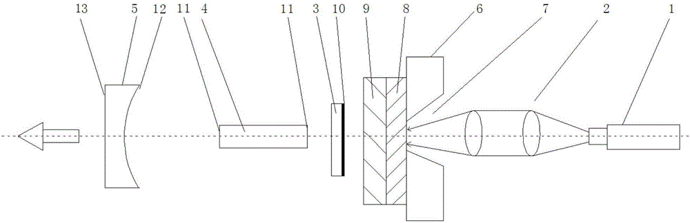
[0025] Back-end pumped miniaturized surface-emitting semiconductor laser in the visible wavelength range, including pump light source 1, collimating and focusing lens group 2, semiconductor gain chip, reflective flat plate 3, and nonlinear crystal from back to front along the optical axis 4 and outcoupling mirror 5;

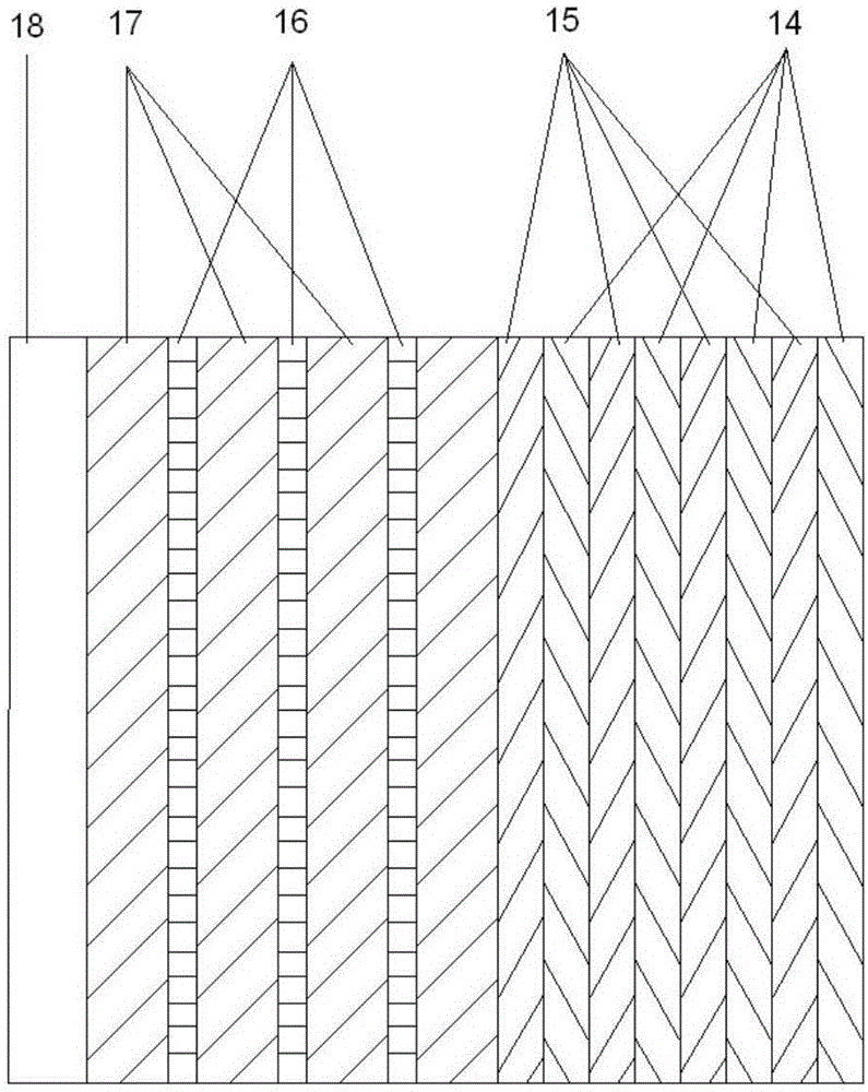
[0026] The semiconductor gain chip is bonded on the heat sink 6 of the bandpass light hole 7; the semiconductor gain chip sequentially includes a first layer with high transmittance to the pump light and high reflectivity to the fundamental frequency infrared laser from back to front. A reflective film 8 and an active region layer 9 for generating a fundamental frequency infrared laser; the nonlinear crystal 4 is used for frequency doubling of the fundamental frequency infrared laser and generating visible light; the reflective flat sheet 3 is inserted in front of the semiconductor gain chip, The reflective flat plate 3 includes a flat plate body and a second ref...

Embodiment 2

[0036] The pump light source is an 808nm semiconductor laser, the collimation and focusing system is a plano-convex lens group with a focal length of 15mm, the heat sink is made of copper material, and the diameters of the large and small circles of the truncated conical aperture are 12mm and 3.5mm respectively.

[0037] The material of the high refractive index layer of the first reflection film in the semiconductor gain chip is Al 0.2 GaAs, the material of the low-refractive index layer is AlAs, and the optical thickness of the two layers is 1 / 4 of the fundamental frequency infrared light wavelength 976nm. The well layer of the quantum well in the active region in the semiconductor gain chip is 8nm thick In 0.13 GaAs material, the barrier layer is GaAs material with a thickness of 130nm. The outermost high barrier layer in the semiconductor gain chip is 207nm thick Al 0.6 GaAs material.

[0038] The rear side of the reflective flat sheet is coated with a second reflective...


PUM


Abstract

The invention discloses a rear end pumped miniaturized visible light wavelength range surface-emitting semiconductor laser comprising a pump light source, a collimating focusing lens group, a heat sink with a light through hole, a semiconductor gain chip, a reflection flat sheet, nonlinear crystal and a coupling output mirror which are arranged from the back to the front along the axial direction of the optical axis. The semiconductor gain chip comprises a reflecting film having high transmittance for the pump light and high reflectance for the fundamental frequency light and a quantum well active region. A film layer having high reflectance for the frequency doubled light and high transmittance for the fundamental frequency light is coated on the rear side of the reflection flat sheet. All the elements are arranged on the same axis which is also the optical axis of the laser resonant cavity so that the quality of the light beams outputted by the laser is enabled to be excellent, adjustment of the device is enabled to be easier than that of any other visible light laser, the mechanical performance of the device is quite stable, the rear end pump mode is combined with the linear structure, the device is enabled to be quite miniature and thus the laser has quite wide application in multiple desktop type comprehensive scientific research instruments.

Description

technical field [0001] The invention specifically relates to a back-end pumped miniaturized visible light wavelength range surface-emitting semiconductor laser, which belongs to the field of semiconductor lasers and relates to the surface-emitting laser technology in semiconductor lasers. This type of laser has the characteristics of excellent beam quality. The invention also relates to nonlinear frequency conversion, in particular to intracavity frequency doubling technology. Background technique [0002] Because the human eye and most detection instruments respond to visible light wavelengths, visible light lasers are among the most versatile lasers. [0003] Existing visible light lasers include gas, solid and semiconductor visible light lasers. Gas visible light lasers, such as helium-neon red lasers, have a single wavelength, low power, complex circuits, and high-voltage parts, which are inconvenient to use. Solid-state visible light lasers are frequency-doubled laser...

Claims


Application Information

Patent Timeline
Patent Type & Authority Applications(China)
IPC IPC(8): H01S5/183
CPCH01S5/18361
Inventor 张鹏朱仁江蒋茂华张丁可崔玉亭
Owner CHONGQING NORMAL UNIVERSITY
Why Eureka
Try Eureka