Novel GaN heterojunction field effect transistor

A heterojunction field effect, transistor technology, applied in semiconductor devices, electrical components, circuits, etc., can solve the problems of threshold voltage hysteresis, weakened control, increased on-resistance, etc., to reduce the maximum peak electric field, reduce Leakage current, the effect of improving breakdown voltage

Inactive Publication Date: 2018-01-23
UNIV OF ELECTRONICS SCI & TECH OF CHINA
View PDF4 Cites 6 Cited by
  • Summary
  • Abstract
  • Description
  • Claims
  • Application Information

AI Technical Summary

Problems solved by technology

[0005] 2. In recent years, the research work of enhanced GaN HEMT has made great progress, but the threshold voltage of enhanced GaN HEMT is relatively low (mostly less than 1V), and the performance is obviously worse than that of depletion-type HEMT.
[0007] (1) Reducing the Al composition or growing a thin barrier layer reduces the 2DEG concentration in the channel, but increases the parasitic resistance and on-state resistance of the AlGaN / GaN HEMT, so the Al composition and barrier layer thickness can only be limited reduced within the range, the threshold voltages are relatively low
[0008] (2) Growth of p-cap capping layer to achieve enhanced HEMT, but the capping layer weakens the control of the gate to the channel, reduces the transconductance of the device, which is not good for high-frequency work, and P-cap technology will introduce P-N junction When the device is working, a large number of holes will be injected into the channel, which will generate a large gate current, resulting in a series of problems such as threshold voltage hysteresis and reliability reduction.
[0009] (3) Recessed gate etching can effectively deplete the 2DEG concentration under the gate, but recessed gate etching requires precise control of the etching depth and will introduce serious etching damage
[0010] 4F-based plasma processing is a promising approach to realize enhanced HEMTs, but introduces injection damage, threshold voltage hysteresis, and high-voltage operation stability issues
However, this technology cannot completely deplete the two-dimensional electron gas in the channel, and cannot give full play to the withstand voltage advantages of GaN materials. At the same time, the deep energy level traps introduced by impurities such as carbon and iron will cause such as increased on-resistance, decreased output current, Negative effects such as current collapse effect and decreased reaction speed

Method used


Image

  • Novel GaN heterojunction field effect transistor
  • Novel GaN heterojunction field effect transistor
  • Novel GaN heterojunction field effect transistor

Examples


Embodiment Construction

[0037] specific implementation plan

[0038] The present invention has been described in detail in the part of the summary of the invention, and will not be repeated here. In order to further illustrate the feasibility of the scheme of the present invention in practical application, the manufacturing process that can prepare the structure of the present invention is proposed below:

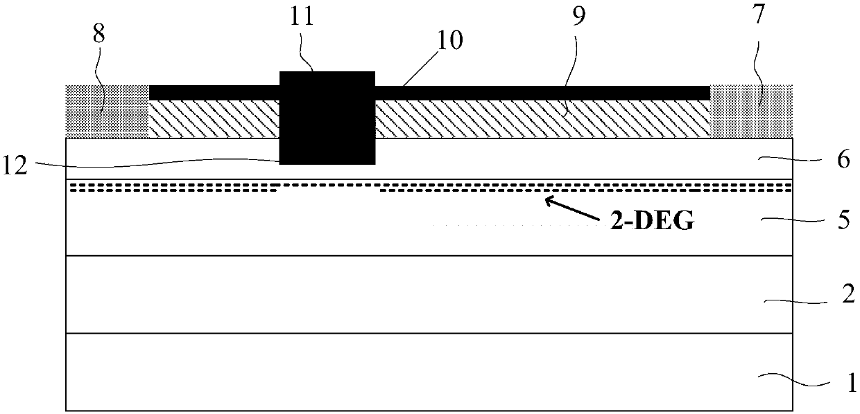
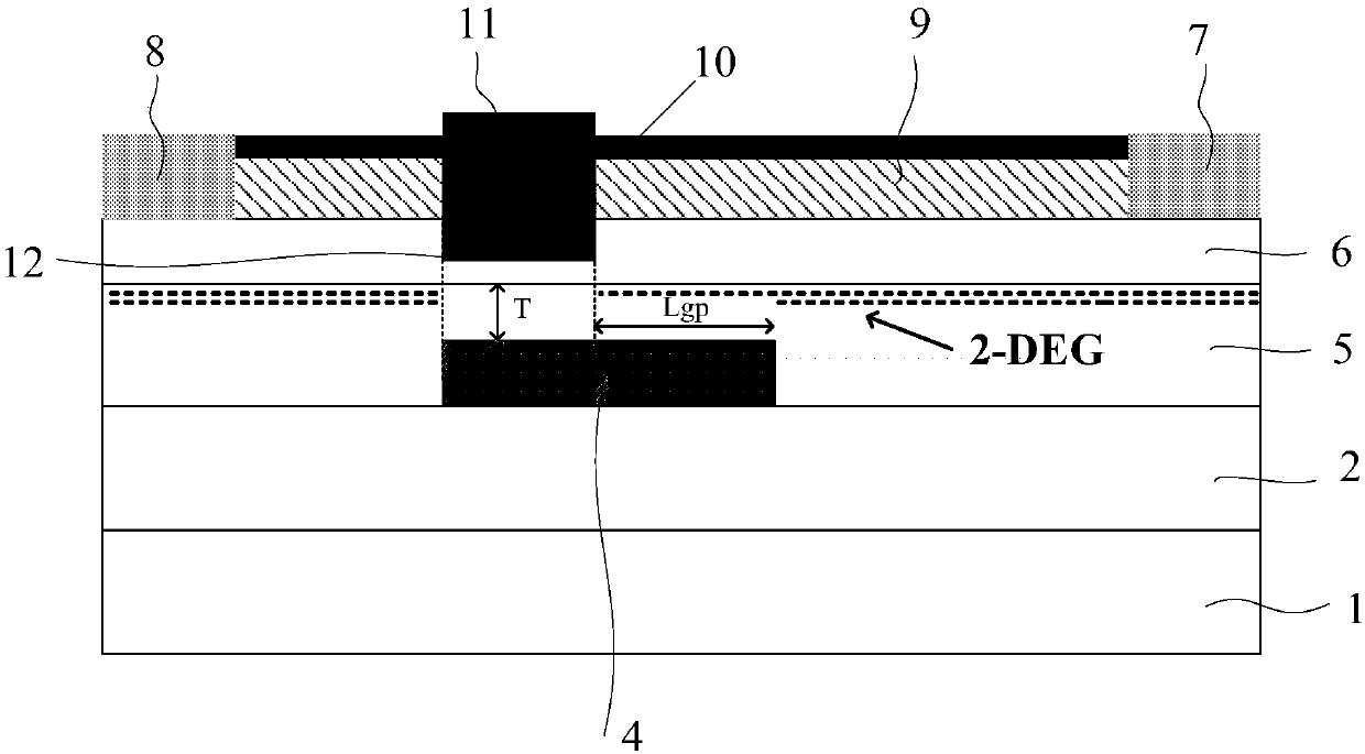
[0039] On a Si, SiC, sapphire or GaN substrate 1, a GaN nucleation buffer layer 2 and a P-type GaN buried layer 3 are sequentially grown by metal-organic chemical vapor deposition (MOCVD) or molecular beam epitaxy (MBE), such as Figure 8 ;

[0040] Etching the P-type GaN buried layer 3 into a local P-type GaN buried layer 4 by using one or a combination of dry etching and oxidation wet etching, such as Figure 9 ;

[0041] The i-type or n-type GaN channel layer 5 and the heterojunction barrier layer 6 are epitaxially grown in sequence by the method of secondary epitaxy, and the evaporation of ...


PUM


Abstract

The invention discloses a novel GaN heterojunction field effect transistor. According to the invention, a P-type GaN buried layer is introduced into a local area of a GaN channel layer of a field effect transistor. The P-type GaN buried layer can improve the heterojunction energy band of the area so as to reduce local channel 2-DEG concentration and a pn junction field board is introduced into theGaN channel layer along the current direction so as to modulate channel electric field. According to the invention, P-type GaN buried layer and groove technology are combined together, so that a threshold value voltage regulation scheme becomes more flexible and threshold value voltage regulation of a larger range can be realized. At the same time, by the electric field modulation effect of the P-type GaN buried layer in the GaN channel layer, the maximal peak value electric field in a device can be reduced effectively and electric field distribution uniformity can be improved. Besides, the P-type GaN buried layer introduces a barrier in a GaN Buffer, so that source and drain electrode punchthrough of the device caused by Buffer electric leakage can be inhibited effectively. Therefore, compared with a traditional groove gating GaN heterojunction field effect transistor, the new structure enlarges the threshold value voltage regulation range effectively and improves the voltage resistance of the device substantially.

Description

technical field [0001] The invention belongs to the technical field of power semiconductors, and relates to a novel GaN heterojunction field effect transistor. Background technique [0002] Due to the limitations of the first two generations of semiconductor materials represented by Si and GaAs, the third generation of wide bandgap semiconductor materials has been developed rapidly because of its excellent performance. Gallium nitride (GaN) material is one of the cores of the third-generation semiconductor materials. Compared with Si, GaAs and silicon carbide (SiC), the special feature is that it has a polarization effect. Due to the polarization effect of the AlGaN / GaN heterojunction, a two-dimensional electron gas conduction channel with high concentration and high electron mobility is generated at the heterojunction interface close to the GaN side, which makes the AlGaN / GaN HEMT device have small on-resistance and fast switching speed. The characteristics of fast and hig...

Claims


Application Information

Patent Timeline
Patent Type & Authority Applications(China)
IPC IPC(8): H01L29/778H01L29/06
Inventor 周琦魏东张安邦朱若璞董长旭石瑜黄芃王方洲陈万军张波
Owner UNIV OF ELECTRONICS SCI & TECH OF CHINA
Why Eureka
Try Eureka