Low power consumption charge trapping type storage device based on graphene oxide quantum dots and preparation method thereof
A technology of graphene quantum dots and charge trapping, applied in electric solid devices, circuits, electrical components, etc., can solve the problems of high power consumption and high operating voltage, and achieve the effects of low power consumption, long-lasting data storage, and low operating voltage
- Summary
- Abstract
- Description
- Claims
- Application Information
AI Technical Summary
Problems solved by technology
Method used
Image

Examples
Embodiment 1
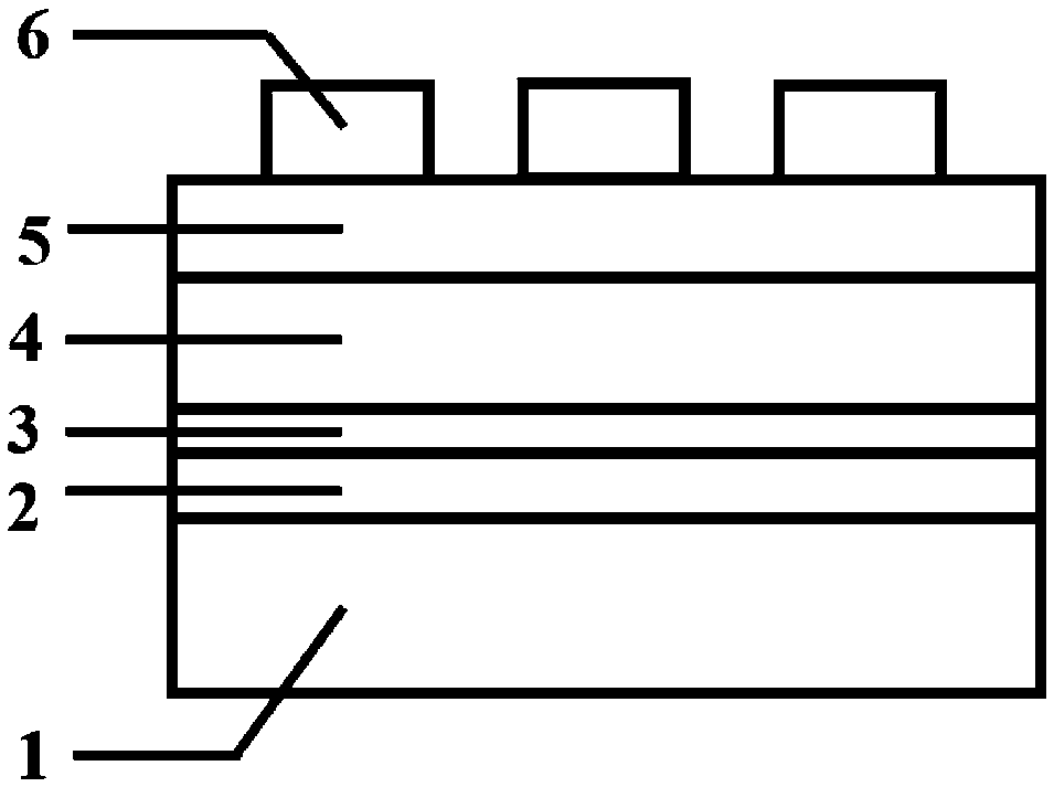
[0035] The charge trapping memory structure prepared by the present invention is as figure 1 As shown, its structure is that SiO is sequentially integrated on Si substrate 1 2 Tunneling layer 2, GQODs / Zr 0.5 f 0.5 o 2 Trapping layer, SiO 2 Barrier layer 5, Pd electrode film layer 6, GQODs / Zr 0.5 f 0.5 o 2 The trapping layer consists of GQODs layer 3 and Zr 0.5 f 0.5 o 2 layer 4, and the GQODs layer 3 is a single-layer graphene oxide quantum dot layer.
[0036] Si substrate 1 is p-type Si material with 100 crystal orientation; SiO 2 The thickness of tunneling layer 2 is 2~5nm; GQODs / Zr 0.5 f 0.5 o 2 The trapping layer 4 has a thickness of 5-80nm, preferably 10-40nm; SiO 2 The barrier layer 5 has a thickness of 5-50 nm, most preferably 5-20 nm; the Pd electrode film layer 6 is a circular electrode film with a thickness of 20-150 nm and a diameter of 60-300 μm.
Embodiment 2
[0038] The preparation method of the charge trapping memory of the present invention, the steps are as follows:
[0039] (a) The p-Si substrate was cleaned with ultrasonic waves in acetone, alcohol and deionized water in sequence, and then washed with HF solution (volume ratio H 2 O:HF=2:1) wash for 2min, then ultrasonically clean with deionized water, take it out and use N 2 Blow dry; put the processed silicon substrate into a high-temperature annealing furnace, and anneal and grow SiO in an oxygen environment 2 Tunneling layer: first use 20s to rise from room temperature to 200°C, 60s to rise from 200°C to 500°C, keep at 500°C for 150s, 10s to drop to 100°C, 40s to drop from 100°C to room temperature, the obtained SiO 2 The thickness of the tunneling layer is 3nm, resulting in SiO 2 / Si structure substrate.
[0040] (c) SiO 2 The / Si structure substrate is placed on the rotating suction cup of the SC-1B homogenizer, and the rotation speed is set to 4000r / min. Use a rub...
PUM
| Property | Measurement | Unit |
|---|---|---|
| Thickness | aaaaa | aaaaa |
| Thickness | aaaaa | aaaaa |
| Thickness | aaaaa | aaaaa |
Abstract
Description
Claims
Application Information
 - R&D
- Intellectual Property
- Life Sciences
- Materials
- Tech Scout
- Unparalleled Data Quality
- Higher Quality Content
- 60% Fewer Hallucinations
Browse by: Latest US Patents, China's latest patents, Technical Efficacy Thesaurus, Application Domain, Technology Topic, Popular Technical Reports.
© 2025 PatSnap. All rights reserved.Legal|Privacy policy|Modern Slavery Act Transparency Statement|Sitemap|About US| Contact US: help@patsnap.com