Method for manufacturing thin film on substrate

A substrate and thin film technology, applied in the field of thin film manufacturing, can solve problems such as poor uniformity, increased operating costs, and high safety requirements, and achieve the goal of increasing the dielectric constant and loss factor, improving energy absorption efficiency, and increasing the number of nuclei Effect

Inactive Publication Date: 2018-03-09
SHENYANG SILICON TECH
View PDF7 Cites 3 Cited by
  • Summary
  • Abstract
  • Description
  • Claims
  • Application Information

AI Technical Summary

Problems solved by technology

If there is a difference in the thermal expansion coefficients of the two bonded materials, it is easy to generate a huge thermal stress at high temperature and destroy the bonded structure of the two materials; The bonded structure is broken due to excessive thermal stress;
[0009] (3) The thermal efficiency of converting thermal energy into kinetic energy by means of annealing is low, and a large amount of external energy must be consumed to carry out, increasing operating costs;
[0013] (1) Due to the poor ...

Method used


Image

  • Method for manufacturing thin film on substrate
  • Method for manufacturing thin film on substrate
  • Method for manufacturing thin film on substrate

Examples


Embodiment 1

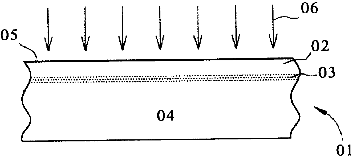
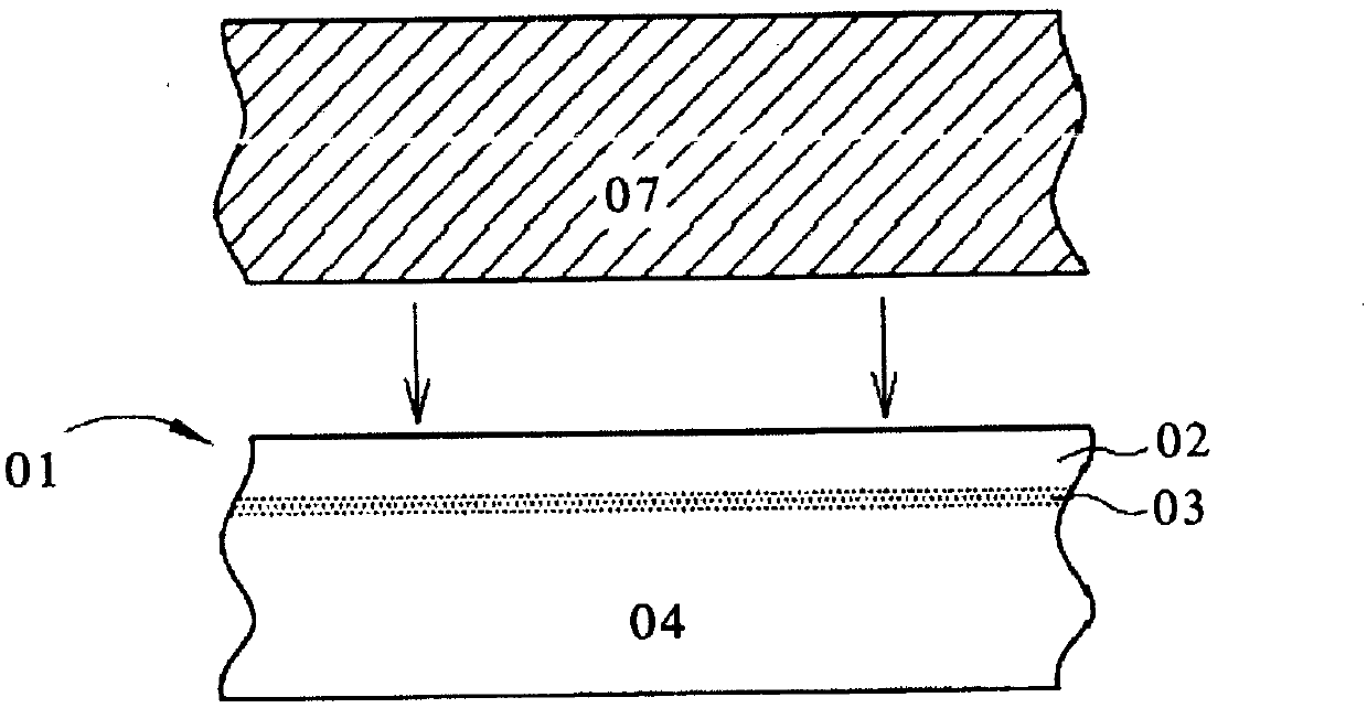
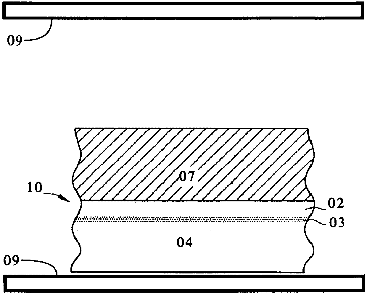
[0081] The original substrate is P-type, the lattice direction is (100), the resistance value is 10-50ohm-cm, and the surface coverage Silicon dioxide (SiO 2 ), single-sided polished, 8″ silicon wafer, dosed at 4.0×10 16 / cm 2 , the implantation energy is 200KeV, hydrogen molecular ions (H 2 + )injection. The target substrate is P-type, the lattice direction is (100), the resistance value is 10-50ohm-cm, and the silicon wafer is polished on one side. Two silicon wafers were bonded into a bonded structure by plasma-enhanced bonding at room temperature, placed in a commercial adjustable power laser cavity, annealed at a temperature of 100-250°C for ten minutes, and then pressed Then at this temperature, the reciprocal of the wavelength corresponding to the selected laser is used as the center frequency. After 1 to 5 minutes of laser irradiation, a layer of silicon film is separated from the original substrate and transferred to the target substrate with a thickness of abou...

Embodiment 2

[0083]The original substrate is P-type, the lattice direction is (100), the resistance value is 10-50ohm-cm, single-sided polishing, 8″ silicon wafer, after two hydrogen molecular ions (H 2 + ) implantation process, the implantation temperature of the first hydrogen molecule ion implantation is 550°C, and the dose is 1.0×10 16 / cm 2 , the implantation energy is 200KeV; followed by the second hydrogen molecular ion implantation, the implantation temperature is room temperature, and the dose is 4×10 16 / cm 2 , the injection energy is 200KeV. The target substrate is a single-sided polished glass wafer. Two silicon wafers are bonded into a bonded structure by plasma-enhanced bonding at room temperature, placed in a commercial laser cavity with adjustable power, annealed at a temperature of 100-250°C for ten minutes, and then pressed Then at this temperature, the reciprocal of the wavelength corresponding to the selected laser is used as the center frequency. After 1 to 5 minu...

Embodiment 3

[0085] The original substrate is P-type, the crystal lattice direction is (100), the resistance value is 10-50 ohm-cm, the silicon wafer is polished on one side, and ion implantation is performed twice. First inject a dose of 1×10 14 / cm 2 , the implantation energy is 180KeV, boron ions (B + ); followed by an injection dose of 5×10 16 / cm 2 , the implantation energy is 129KeV, hydrogen molecular ions (H 2 + ). The target substrate is a single-sided polished glass wafer. The two wafers are bonded into a bonded structure by plasma-enhanced bonding at room temperature, placed in a commercial laser cavity with adjustable power, and annealed at a temperature of 100-250°C for ten minutes in the cavity, and then followed by At this temperature, the reciprocal of the wavelength corresponding to the selected laser is used as the center frequency. After 1 to 5 minutes of laser irradiation, a layer of silicon film is separated from the original substrate and transferred to the tar...


PUM

PropertyMeasurementUnit
Thicknessaaaaaaaaaa

Abstract

The present invention provides a method for manufacturing a thin film on a substrate. The method comprises the following steps that: an original substrate is provided; an ion separation layer is formed in the original substrate by using an ion implantation method, so that a thin film layer and a remaining medium layer can be formed on the original substrate through the ion separation layer, wherein the thin film layer is a region for bearing ion implantation in the original substrate, and the remaining medium layer is a region where no ions are implanted; a target substrate is bonded to the original substrate through a wafer bonding method, so that the target substrate and the original substrate can be bonded to a bonded structural body; and the bonded structural body is heated, and laseris adopted to irradiate the bonded structural body, so that the thin film layer and the remaining medium layer can be separated from each other, and the thin film layer can be transferred from the original substrate to the target substrate, and the heating temperature of the bonded structural body is higher than room temperature and conversion temperature that enables the dielectric constant and loss factor of the bonded structural body to be converted, and is lower than temperature that activates a smart cut method.

Description

technical field [0001] The invention relates to a method for manufacturing a thin film on a substrate, in particular to a method for transferring a thin film having the same area as the original substrate, nanoscale thickness, high film thickness uniformity, and low defect density. Background technique [0002] The wafer bonding method can combine two single-crystal wafers with very different lattice constants. The bonding interface in the middle does not need to use any glue and remains completely clean, but still can obtain the same bonding strength as the substrate To meet the strict requirements of electronic and optoelectronic materials for interface properties. [0003] In 1988, Dr. W. Maszara in the United States applied a P + Type Etch StopLayer (Etch StopLayer), to make sub-micron-thick bonded insulating layer silicon wafer (Bonding Etch-Back Silicon onInsulator; BESOI), making the application of this technology (BESOI) expanded to electronic materials, optoelectro...

Claims


Application Information

Patent Timeline
IPC IPC(8): H01L21/02H01L21/20H01L21/265
CPCH01L21/02656H01L21/2007H01L21/265
Inventor 李捷
Owner SHENYANG SILICON TECH
Why Eureka
Try Eureka