Thick high-conductivity multilayer graphene film and RFID electronic label of impedance loaded shape

A multi-layer graphene, high-conductivity technology, applied in the field of antenna technology and radio frequency identification, can solve the problems of insufficient mechanical flexibility and corrosion resistance of metal antennas, complicated manufacturing process, and many antenna materials, and reduce the number of processes. The effect of manufacturing errors, reducing material consumption, and improving yield

Inactive Publication Date: 2018-03-23
WUHAN UNIV OF TECH
View PDF5 Cites 7 Cited by
  • Summary
  • Abstract
  • Description
  • Claims
  • Application Information

AI Technical Summary

Problems solved by technology

At present, the antenna material of most radio frequency identification electronic tags is copper, aluminum, silver paste or conductive ink. Some deficiencies in mechanical flexibility and corrosion resistance

Method used


Image

  • Thick high-conductivity multilayer graphene film and RFID electronic label of impedance loaded shape
  • Thick high-conductivity multilayer graphene film and RFID electronic label of impedance loaded shape
  • Thick high-conductivity multilayer graphene film and RFID electronic label of impedance loaded shape

Examples


Embodiment 1

[0029] 1) Polyimide, polyamide, and graphene oxide are formed into films by doctor blade method or screen printing method, and hot-pressed at 180°C to obtain a graphene film precursor;

[0030] 2) placing the obtained graphene film precursor in a high-temperature furnace in an inert gas or vacuum environment, first heat-treating at 500°C for 2 hours at a low temperature, then heat-treating at 1500°C for 3 hours and 2800°C for 3 hours;

[0031] 3) Repeat the heat treatment cycle described in step 2 for more than 3 times; then drop the temperature to room temperature at a constant rate of 4°C per minute; further roll forming at room temperature to obtain a high-conductivity multilayer graphene thick film.

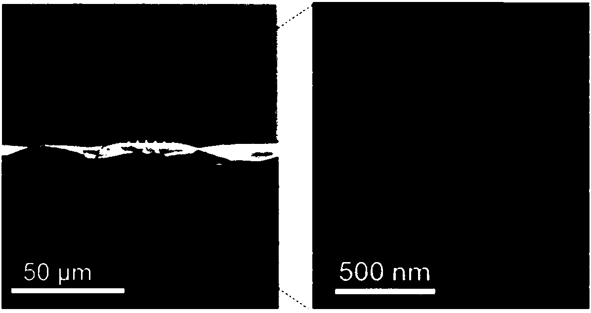
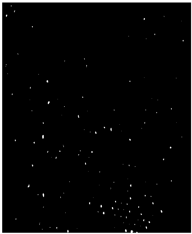
[0032] The microstructure and morphology of the graphene thick film were characterized by scanning electron microscope and transmission electron microscope: figure 1 It is the cross-section of the graphene thick film and the enlarged scanning electron microscope image, it can...

Embodiment 2

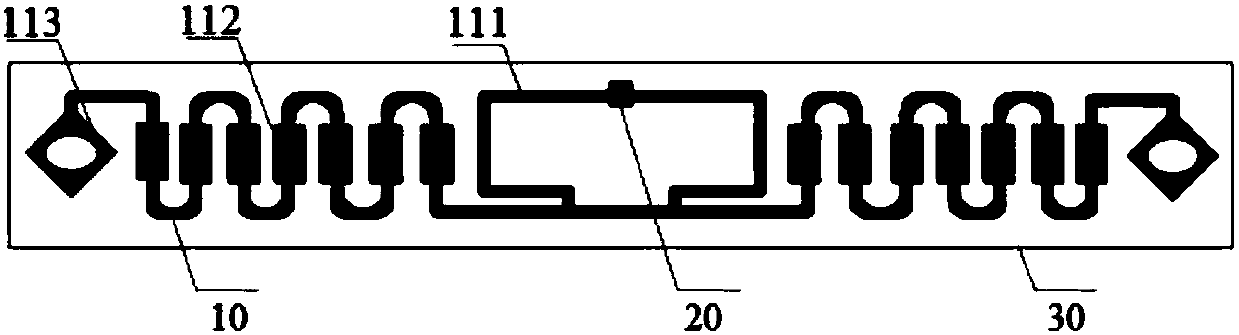
[0035] refer to Figure 4 In this embodiment, the high-conductivity multi-layer graphene thick film and the impedance-loaded high-frequency radio frequency electronic identification tag include an antenna 10, a chip 20, and a substrate 30, covering a frequency band of 13.56 MHz. Described antenna 10 comprises impedance loading shape coil 121, bridge 122 and via hole 123, and its material is high-conductivity multilayer graphene thick film, and thick film conductivity is 1×10 6 S / m, the number of layers is about 75,000 layers, which is formed by preparing a large thick film in the film forming step in Example 1 and then pressing it mechanically. The impedance-loaded coil is square, the coil width is 0.5 mm, and the number of coils is 8 turns. The chip model is NXPMFRC522. The substrate 30 is arranged in a rectangular shape, made of PVC, and its size range is 100mm in length, 90mm in width, and 0.2mm in thickness.

Embodiment 3

[0037] refer to Figure 5 In this embodiment, the high-conductivity multilayer graphene thick film and the impedance-loaded microwave-band radio frequency electronic identification tag include an antenna 10, a chip 20, and a substrate 30, covering a frequency band of 2.45 GHz. The material of the antenna 10 is a high-conductivity multilayer graphene thick film, and the conductivity of the thick film is 8×10 5 S / m, the number of layers is about 60,000, and it is directly prepared by the film-forming step in Example 1. The left arm of the dipole is an impedance-loaded linear dipole 131 with an arm length of 50 mm, and the right arm and the left arm are mirror images. The chip model is nRF2401. The substrate 30 is arranged in a rectangular shape, made of PET, and its size range is 120 mm in length, 20 mm in width, and 0.3 mm in thickness.


PUM

PropertyMeasurementUnit
electrical conductivityaaaaaaaaaa

Abstract

The invention discloses a thick high-conductivity multilayer graphene film and an RFID electronic label of an impedance loaded shape. A graphite film precursor including polyimides, polyamide and oxidized graphene forms a film in a scraping or screen printing method, and a graphene film precursor is prepared by hot press molding at the temperature of 50-180 DEG C; the graphene film precursor is placed in a high temperature furnace, heat treatment at the low temperature of 200-500 DEG C for 1-2 hours, heat treatment at 200-500 DEG C for 2-5 hours and heat treatment at 2000-2800 DEG C for 2-5 hours are carried out on the graphene film precursor successively in a cyclic way, and the graphene film precursor is then cooled for 12 hours slowly; and roll forming is carried out. Compared with a traditional metal material, the prepared RFID electronic label has similar functions, a signal transmission performance is ensured, the label can be produced in large scale to reduce the cost, and unique properties as high temperature resistance, corrosion resistance, flexibility and environmental protection of a graphene material are included.

Description

technical field [0001] The invention belongs to the field of antenna technology and radio frequency identification, in particular to a high-conductivity multilayer graphene thick film and an impedance-loaded radio frequency identification electronic tag. Background technique [0002] Radio frequency identification (RFID) is an automatic identification technology that conducts non-contact two-way data communication through radio frequency, identifies targets and obtains relevant data. With the popularization of the Internet of Things, radio frequency identification is widely used in daily life fields such as logistics, food traceability, medical management, and access control. A large number of articles and patents focus on the design of the antenna, in order to enable the tag to transmit longer distances and cope with more complex environments. At present, the antenna material of most radio frequency identification electronic tags is copper, aluminum, silver paste or conduc...

Claims


Application Information

Patent Timeline
Patent Type & Authority Applications(China)
IPC IPC(8): H01Q1/36H01Q1/38H01Q7/00H01Q9/20H01Q9/28H01Q1/22G06K19/07G06K19/077
CPCG06K19/0723G06K19/07722G06K19/07749H01Q1/2225H01Q1/368H01Q1/38H01Q7/00H01Q9/20H01Q9/285
Inventor 吴志鹏何大平张博涵
Owner WUHAN UNIV OF TECH
Why Eureka
Try Eureka