Sn2Nb2O7 Photo-anode material and Sn2Nb2O7 photoelectrode film

A photoanode and photoelectrode technology, applied in the field of photoelectrochemistry, can solve the problems of photoelectrochemical performance of photoanode materials, and achieve the effects of alleviating environmental energy shortage, good optical characteristics, and simple preparation methods

Pending Publication Date: 2018-05-04
LIAONING UNIVERSITY
View PDF5 Cites 7 Cited by
  • Summary
  • Abstract
  • Description
  • Claims
  • Application Information

AI Technical Summary

Problems solved by technology

So far, for Sn 2 Nb 2 o 7 There are very few studies on semiconductor materials, and...

Method used


Image

  • Sn2Nb2O7 Photo-anode material and Sn2Nb2O7 photoelectrode film
  • Sn2Nb2O7 Photo-anode material and Sn2Nb2O7 photoelectrode film
  • Sn2Nb2O7 Photo-anode material and Sn2Nb2O7 photoelectrode film

Examples


Embodiment 1

[0023] Example 1 Sn 2 Nb 2 o 7 photoanode material

[0024] (1) Preparation method

[0025] By SnO and Nb 2 o 5 The solid-to-liquid ratio of the mixture to ethanol is 1g: 2ml, take 7.5mmol of SnO and 5mmol of Nb 2 o 5 Mix in ethanol, as for the ball mill tank, the grinding balls in the tank are 265g; start the ball mill, set the speed at 200 r / min, grind for 14h, turn off the power, wash with ethanol and dry, and dry the powder in the Annealing treatment at 900°C for 4 hours in a muffle furnace, cooling to room temperature, and obtaining Sn 2 Nb 2 o 7 powder.

[0026] (2) Detection

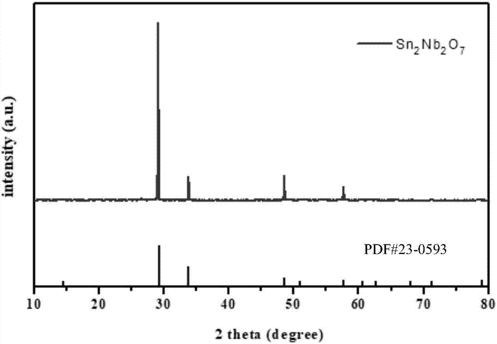
[0027] will get Sn 2 Nb 2 o 7 Powder carries out XRD test, the result is as follows figure 1 shown by figure 1 Visible, Sn 2 Nb 2 o 7 Has good crystallinity.

Embodiment 2

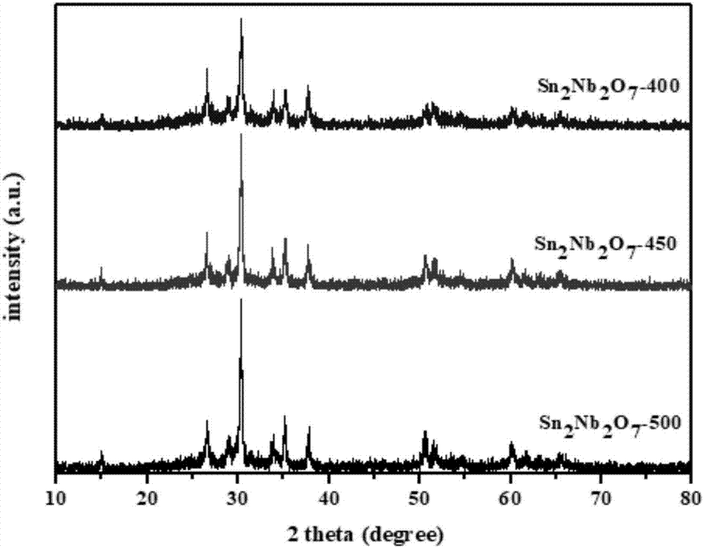
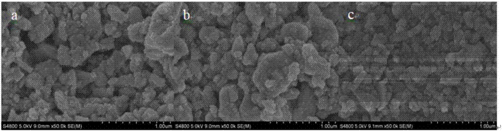
[0028] Example 2 Sn 2 Nb 2 o 7 Photoelectrode film

[0029] (1) Sn 2 Nb 2 o 7 Photoelectrode thin film Sn 2 Nb 2 o 7 -400 preparation

[0030] 1) Take 10mg I 2 Place in 25ml of acetone aqueous solution (the volume ratio of water to acetone is 1:25), seal and sonicate for 60min until the solution is uniformly dispersed, and the mixture containing I 2 of acetone solution.

[0031] 2) get the Sn prepared by 0.1g embodiment 1 2 Nb 2 o 7 Powder dispersed in containing I 2 In the acetone aqueous solution, sealed and sonicated for 90min, the electrophoretic deposition suspension was obtained.

[0032] 3) Two transparent conductive glasses (FTO) with equal areas are immersed in the electrophoretic deposition suspension parallel to each other face to face, and a DC voltage of 20V is applied between the two electrodes, and deposited for 1 min.

[0033] 4) Cut off the current, take the transparent conductive glass (FTO) out of the suspension, dry it at room temperature, and...

Embodiment 3

[0040] Example 3 Sn 2 Nb 2 o 7 Application of Photoelectrode Thin Film

[0041] The Sn prepared by embodiment 2 was respectively 2 Nb 2 o 7 -400, Sn 2 Nb 2 o 7 -450 and Sn 2 Nb 2 o 7 -500 photoelectrode thin films are used for photoelectrochemical performance tests such as photocurrent, impedance, and quantum efficiency.

[0042] All electrochemical experiments were carried out in an electrochemical workstation (Princeton Applied Research 2273) with a three-electrode system. The sample film is used as the working electrode, the platinum sheet is used as the counter electrode, Ag / AgCl is used as the reference electrode, the electrolyte is 0.5M sodium sulfate, and the light irradiation area of ​​the sample is 1cm 2 .

[0043] Photocurrent test: the light source is 300W xenon lamp, the bias voltage is 1.18V vs.V RHE , the measured results are as Figure 4 As shown, the results show that the firing temperature has an effect on the photocurrent, and the photocurren...


PUM


Abstract

The invention discloses a Sn2Nb2O7 photo-anode material and a Sn2Nb2O7 photoelectrode film. Sn2Nb2O7 powder is prepared with SnO and Nb2O5 via a solid reaction process and is used as a raw material; the raw material is made into a film electrode by electrophoretic deposition; Sn2Nb2O7 photoelectrode film is calcined to obtain an electrode film of good crystallinity; Sn2Nb2O7 is a multicomponent metal oxide, energy band of Sn2Nb2O7 may cross a conduction band and valence band of water, Sn2Nb2O7 is suitable for water decomposition and has stable properties in aqueous solutions as well as good photochemical properties, and a preparation method is simple. Studies on Sn2Nb2O7 provide novel catalytic materials for water decomposition, studies on renewable energy are benefited, and the severe condition of current environmental energy tension is relieved.

Description

technical field [0001] The invention belongs to the technical field of photoelectrochemistry, in particular to a new photoanode material Sn 2 Nb 2 o 7 and its application. Background technique [0002] Photoelectrochemical water splitting to produce hydrogen, which converts solar energy into storable chemical energy, is the main means to solve environmental and energy problems in the 21st century. The development of photoanode materials is the key to realize the large-scale application of photoelectrochemical water splitting. As an ideal photoanode semiconductor material, it must have the characteristics of suitable band gap, conduction band and valence band energy level, effective carrier transport, good stability and low cost. However, no photoanode material that can simultaneously satisfy the above requirements has been found so far. Therefore, it is imperative to improve the performance of existing semiconductor materials and develop new photoanode materials with ap...

Claims


Application Information

Patent Timeline
IPC IPC(8): H01L51/44H01G9/042
CPCH01G9/042H10K30/81Y02E10/549
Inventor 范晓星刘京王绩伟韩东远王晓娜
Owner LIAONING UNIVERSITY
Why Eureka
Try Eureka