Laminated solar cell

A solar cell and stacking technology, applied in the field of solar cells, can solve the problems of high requirements for experimental equipment, high manufacturing costs, and high equipment requirements

Pending Publication Date: 2018-05-18
深圳市远信储能技术有限公司
View PDF0 Cites 5 Cited by
  • Summary
  • Abstract
  • Description
  • Claims
  • Application Information

AI Technical Summary

Problems solved by technology

[0002] The efficiency of CdTe cells has developed rapidly in recent years. The highest conversion efficiency of 22.1% was set by First Solar in the United States in 2016, but it faces the problems of high equipment requirements and high manufacturing costs.
One of the factors affecting the efficiency of CdTe cells is the thickness of the cadmium sulfide (CdS) window layer. In order to reduce the light absorption loss, the thickness of CdS with a bandgap width of 2.4eV should be as thin as possible in theory, generally less than 100nm. However, in the actual process Pinholes in the thick CdS film and non-conformal coverage on the transparent conductive oxide film can lead to leakage, which can lead to poor battery performance
In order to prepare high-efficiency CdTe batteries, there are strict requirements on the thickness of CdS: not only the thickness of CdS film is required to be less than 100nm, but also the film must not leak electricity on the transparent conductive film, so the requirements for experimental equipment are high, and the preparation cost is high.

Method used


Image

  • Laminated solar cell
  • Laminated solar cell
  • Laminated solar cell

Examples


preparation example Construction

[0035] The present invention also provides a method for preparing the above laminated solar cell, comprising:

[0036] S1) Preparation of perovskite battery and cadmium telluride battery.

[0037] The perovskite battery is prepared according to the following steps: a hole transport layer is prepared on the conductive glass by a spin coating method; bromine-doped CH is prepared on the hole transport layer by a spray coating method or a spin coating method. 3 NH 3 PB 3 thin film; in the bromine-doped CH 3 NH 3 PB 3 A PCBM layer is prepared by a spin coating method on the thin film; a transparent electrode is prepared on the PCBM layer by a spray coating method to obtain a perovskite cell.

[0038] The cadmium telluride battery is prepared according to the following steps: a cadmium sulfide buffer layer is prepared on the conductive glass by a chemical water bath method or a magnetron sputtering method; a magnetron sputtering method or a near-space sublimation method is used...

Embodiment 1

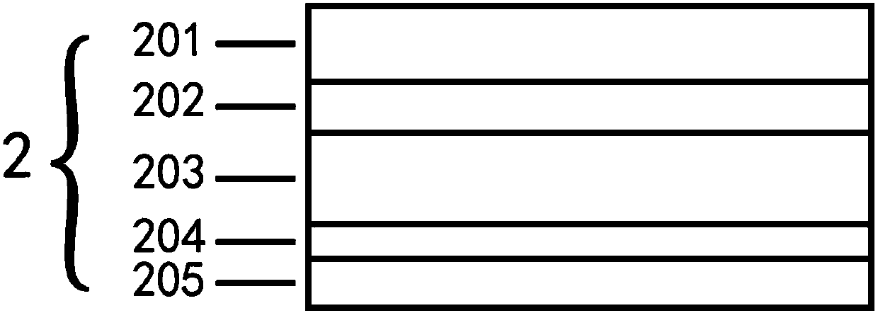
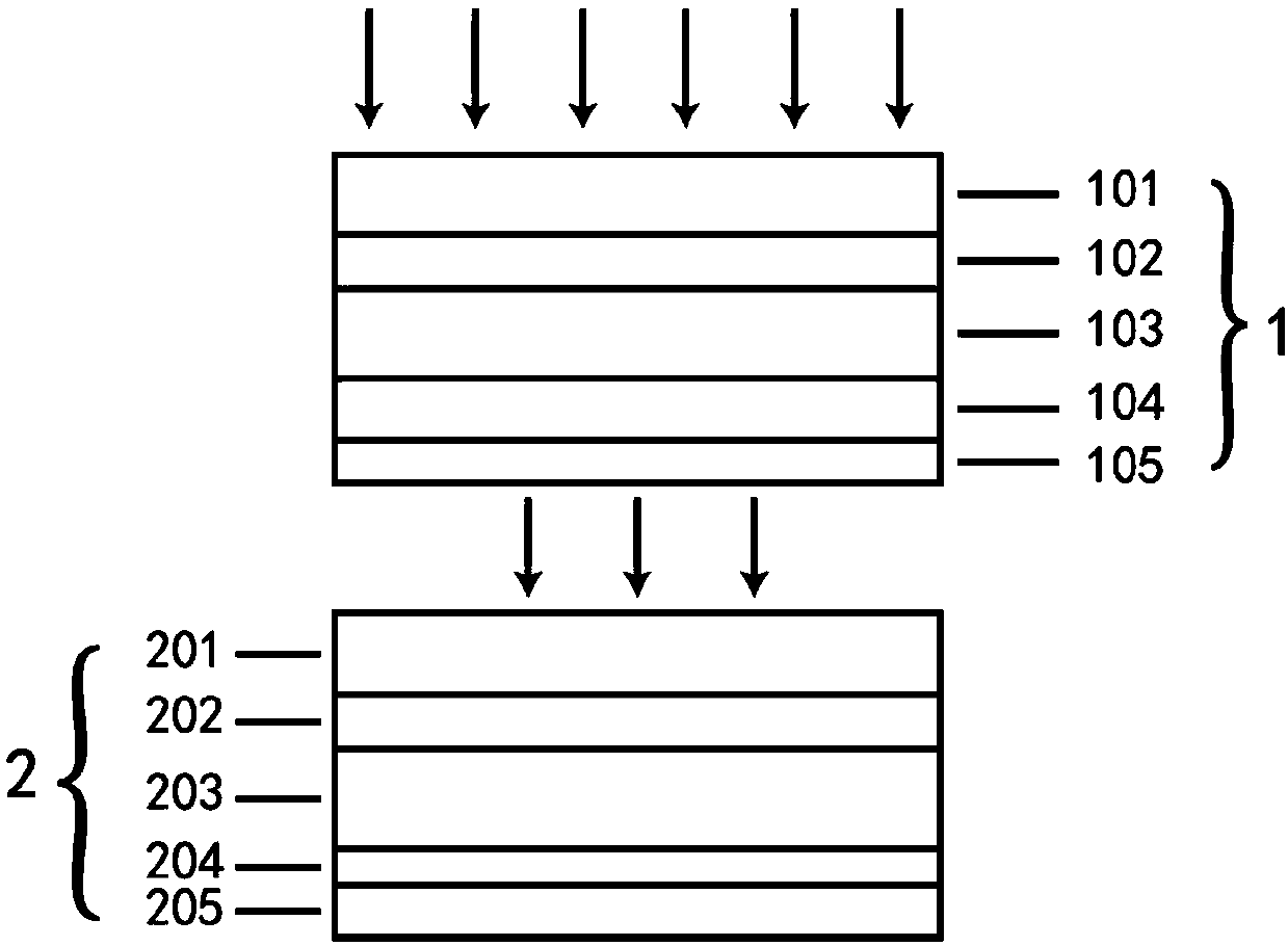
[0044] see figure 1 and figure 2 ; figure 1 is a schematic diagram of the structure of a cadmium telluride battery; figure 2 It is a schematic diagram of the structure of a tandem solar cell, in which 1 is a perovskite cell, 101 is a fluorine-doped tin dioxide FTO conductive glass, 102 is a PIF8-TAA hole transport layer, and 103 is a bromine-doped perovskite CH 3 NH 3 Pb(I 1-x Br x ) 3 layer, 104 is the PCBM electron transport layer, 105 is the silver nanowire layer; 2 is the cadmium telluride battery, 201 is the tin dioxide FTO conductive glass doped with fluorine, 202 is the CdS buffer layer, 203 is the CdTe absorption layer, 204 is Copper layer, 205 is a gold layer.

[0045] Preparation of perovskite battery 1:

[0046] (1) A PIF8-TAA hole transport layer 102 is prepared on the fluorine-doped tin dioxide FTO conductive glass 101 by spin coating method, with a thickness of 50-100 nm.

[0047] (2) Preparation of CH by spray coating or spin coating 3 NH 3 Pb(I 1-...

Embodiment 2

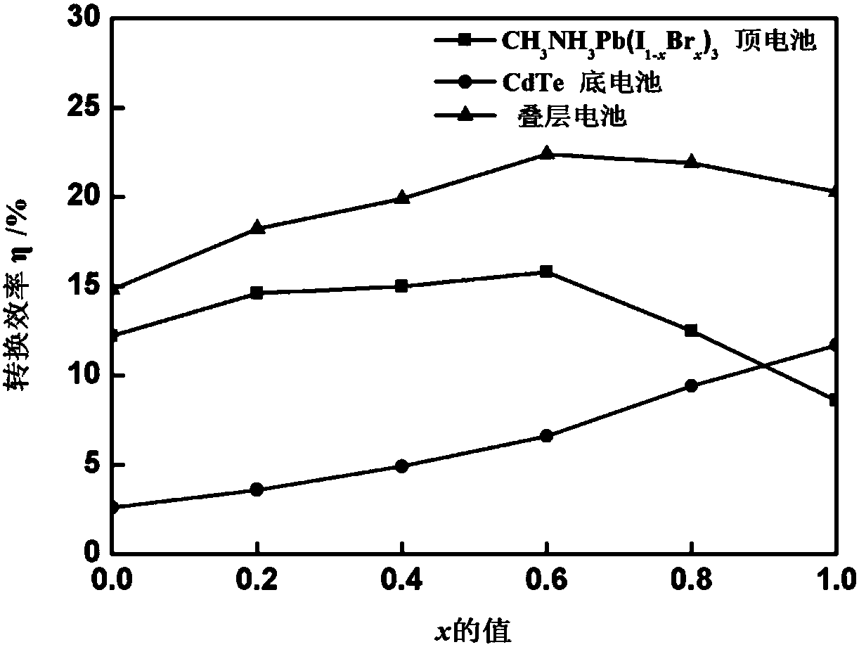
[0056] Laminated battery adopts figure 2 Shown CH 3 NH 3 Pb(I 1-x Br x ) 3 / CdTe stacked solar cell structure. In this structure, light from CH 3 NH 3 Pb(I 1-x Br x ) 3 When the top cell is incident, the shorter wavelength will be absorbed by the top cell to generate photogenerated carriers with higher energy, and the transmitted light will generate photogenerated carriers in the CdTe bottom cell, thus broadening the sensitivity of the two cells to sunlight. Absorb the wavelength range and improve the utilization rate of light.

[0057] in CH 3 NH 3 Pb(I 1-x Br x ) 3 In the top battery, in order to improve the transmittance of the battery, silver nanowires (AgNW) with good conductivity and transparency are selected as electrodes. The characteristic length of silver nanowires is 10-50 microns, the diameter is 20-50nm, and the thickness of silver nanowires is In the range of 100-150nm, the square resistance is 20-50 ohms per square, and the light transmittance i...


PUM


Abstract

The invention provides a laminated solar cell. The solar cell comprises a top cell and a bottom cell which are superposed. The top cell is a perovskite cell. The perovskite cell comprises a bromine doped CH3NH3PbI3 film. The bottom cell is a cadmium telluride cell. Compared with the prior art, by using the cell of the invention, a forbidden bandwidth of the perovskite cell can be changed in a range of 1.57eV to 2.30eV along with a bromine-doped proportion change, a forbidden bandwidth of the cadmium telluride cell is 1.43eV, the perovskite cell is taken as the top cell, the cadmium telluride cell is taken as the bottom cell, and the manufactured laminated cell can widen absorption wavelength ranges of the two cells to sunlight; cell conversion efficiency is increased, and a requirement toa cadmium sulfide thickness is reduced, which is good for reducing manufacturing cost; simultaneously, photon-generated carrier energy generated by light with a short wave length in the perovskite cell of a wide forbidden band is increased and an open-circuit voltage of the laminated cell is increased too.

Description

technical field [0001] The invention belongs to the technical field of solar cells, in particular to a laminated solar cell. Background technique [0002] The efficiency of CdTe cells has developed rapidly in recent years. The highest conversion efficiency of 22.1% was set by First Solar in 2016, but it faces the problems of high equipment requirements and high manufacturing costs. One of the factors affecting the efficiency of CdTe cells is the thickness of the cadmium sulfide (CdS) window layer. In order to reduce the light absorption loss, the thickness of CdS with a bandgap width of 2.4eV should be as thin as possible in theory, generally less than 100nm. However, in the actual process Both pinholes in the CdS film of this thickness and non-conformal coverage on the transparent conductive oxide film lead to leakage, which leads to poor battery performance. In order to prepare high-efficiency CdTe batteries, there are strict requirements on the thickness of CdS: not only...

Claims


Application Information

Patent Timeline
Patent Type & Authority Applications(China)
IPC IPC(8): H01L31/0725H01L31/073H01L51/42H01L25/16
CPCH01L25/167H01L31/0725H01L31/073H10K30/30Y02E10/543Y02E10/549
Inventor 陈乐伍王堉赖其聪王少武
Owner 深圳市远信储能技术有限公司
Why Eureka
Try Eureka