Chip epitaxial structure of low-resistance LED and preparation method thereof

An epitaxial structure and chip technology, applied in the direction of electrical components, circuits, semiconductor devices, etc., can solve the problem of reducing the contact resistance of P-type semiconductor materials/P-type electrodes, increasing hole injection efficiency, and poor hole injection efficiency and other issues, to achieve the effect of improving photoelectric conversion efficiency, improving I-V characteristics, and alleviating the effect of current crowding

Pending Publication Date: 2018-09-14
HEBEI UNIV OF TECH
View PDF1 Cites 6 Cited by
  • Summary
  • Abstract
  • Description
  • Claims
  • Application Information

AI Technical Summary

Problems solved by technology

However, the LED technology of nitride semiconductors still faces the problems of poor hole injection efficiency and low photoelectric conversion efficiency, among which the high contact resistance of semiconductor materials and metal electrodes is an important factor causing low photoelectric conversion efficiency
After research by researchers, it was found that compared with Si-doped N-type nitride semiconductor materials, the activation energy of Mg-doped impurities in P-type semiconductor materials is higher, so the efficiency of P-type doping is also relatively low. , which leads to the problem of low hole concentration, a higher Schottky barrier will be formed at the contact junction between the P-type semiconductor material and the P-electrode, resulting in an increase in contact resistance and hindering the injection of holes
In addition, a higher Schottky barrier and a wider depletion region will also be formed at the contact junction between the N-type semiconductor material and the N-type electrode, resulting in an increase in contact resistance and hindering the injection of electrons. Although heavy doping can be achieved, it is impossible to completely avoid the appearance of the Schottky barrier
In order to reduce the contact resistance of LED devices, researchers, for example, use Sn-purge treatment to reduce the surface roughness of the indium tin oxide contact layer, thereby reducing the contact resistance and conduction voltage, and making the photoelectric conversion efficiency improved. Improvement, this method is only for LEDs with indium tin oxide as the current spreading layer, and the scope of application is narrow (Wbin Tu, Zimin Chen et al. Performance optimization of AlGaN-based LEDs by use of ultraviolet-transparent indium tin oxide:Effect of in situ contact treatment [J]. Applied Physics Express, 2018, 11, 052101); the Chinese patent with the patent number CN105932129A discloses a LED chip structure and its preparation method. The structure is between a P-type semiconductor material and a P-type electrode Inserting an insulating layer between them can increase the hole injection efficiency and reduce the contact resistance of the P-type semiconductor material / P-type electrode

Method used


Image

  • Chip epitaxial structure of low-resistance LED and preparation method thereof
  • Chip epitaxial structure of low-resistance LED and preparation method thereof
  • Chip epitaxial structure of low-resistance LED and preparation method thereof

Examples


preparation example Construction

[0059] A method for preparing a chip epitaxial structure of a low-resistance LED of the present invention, the steps of the method are as follows:

[0060] In the first step, the substrate 101 is baked at a high temperature of 900°C to 1400°C in an MOCVD (metal organic compound chemical vapor deposition) or MBE (molecular beam epitaxy) reaction furnace to remove foreign matter attached to the substrate surface ;

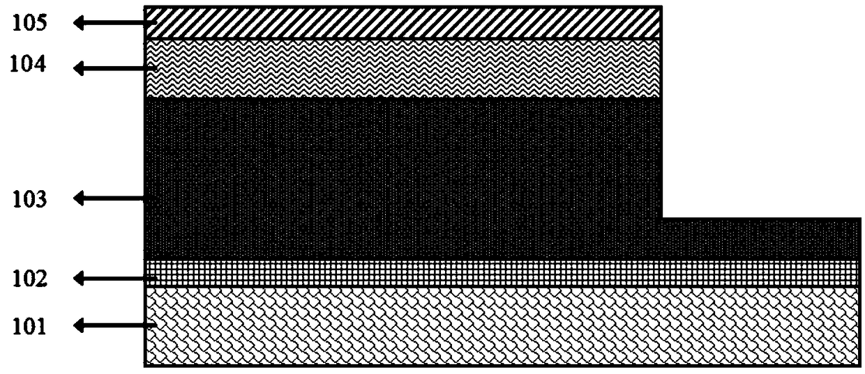
[0061] The second step is to epitaxially grow a buffer layer 102 with a thickness of 10 to 50 nm on the surface of the substrate 101 treated in the first step in an MOCVD or MBE reactor, so as to filter dislocations and release stress caused by lattice mismatch;

[0062] The third step is to deposit an N-type semiconductor material layer 103 with a thickness of 1-5 μm on the buffer layer 102 obtained in the second step in an MOCVD or MBE reactor;

[0063] In the fourth step, in the MOCVD or MBE reaction furnace, epitaxially grow the multi-quantum well layer 104 on t...

Embodiment 1

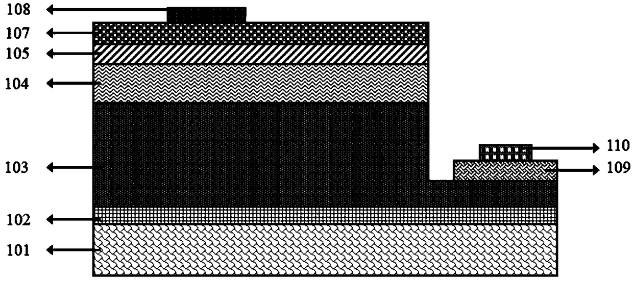
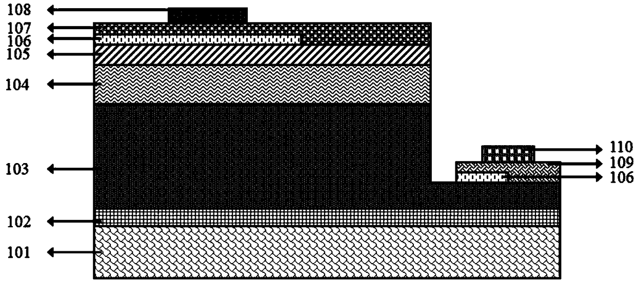
[0072] The present embodiment has a chip epitaxial structure of a low-resistance LED, and the epitaxial structure includes in sequence along the epitaxial growth direction: a substrate 101, a buffer layer 102, an N-type semiconductor material layer 103, a multi-quantum well layer 104, a P- Type semiconductor material layer 105, insulating layer 106, current spreading layer 107, N pole ohmic contact layer 109, P-type ohmic electrode 108 and N-type ohmic electrode 110, wherein the material used for the thickness of insulating layer 106 is SiO 2 , the thickness is 1 nm, the insulating layer 106 on the P-type semiconductor material layer 105 is a 1 / 4 ring, and the width of this ring is 200 μm, and the insulating layer 106 on the N-type semiconductor material layer 103 is a 1 / 2 ring, The ring has a width of 10 μm and is a patterned film structure.

[0073] Among the above, the substrate 101 is sapphire, which grows epitaxially along the [0001] direction; the material of the buffer ...

Embodiment 2

[0089] The components of the chip epitaxial structure of a low-resistance LED in this embodiment are the same as in Embodiment 1, except that the material of the buffer layer 102 is GaN with a thickness of 25nm; the material of the N-type semiconductor material layer 103 is GaN, The thickness is 3 μm; the structure of the multi-quantum well layer 104 is 3 periods of In 0.18 Ga 0.82 N / GaN layer, in which the thickness of the quantum barrier GaN is 10nm, and the quantum well In 0.18 Ga 0.82 The thickness of N is 3nm, and the forbidden band width of quantum barrier is 0.83eV larger than the forbidden band width of quantum well; The material of P-type semiconductor material layer 105 is GaN, and thickness is 60nm; The material of insulating layer 106 is Al 2 o 3 , the thickness is 1.5nm, the insulating layer 106 on the P-type semiconductor material layer 105 is a square, and the side length is 100 μm, and the insulating layer 106 on the N-type semiconductor material layer 103 i...


PUM


Abstract

The present invention provides a chip epitaxial structure of a low-resistance LED and a preparation method thereof. The structure comprises a substrate, a buffer layer, an N-type semiconductor material layer, a multi-quantum well layer, a P-type semiconductor material layer, a current expanding layer and a P-type Ohmic electrode in order in an epitaxial growth direction. The current expanding layer and the N-type semiconductor material layer are respectively embedded with insulation layers. The epitaxial structure further comprises an N-pole Ohmic contact layer and an N-type Ohmic electrode; the N-pole Ohmic contact layer is located on part of the N-type semiconductor material layer; and the N-type Ohmic electrode is located on the N-pole Ohmic contact layer. The preparation method is simple, high in operability and low in cost, can increase the injection efficiency of carriers to a certain extent on the basis of further reduction of the Ohmic contact resistance, and greatly improves the implementation performances.

Description

technical field [0001] The technical solution of the invention relates to a semiconductor device specially suitable for light emission with at least one potential jump barrier or surface barrier, specifically a chip epitaxial structure of a low-resistance LED and a preparation method thereof. Background technique [0002] Energy saving and environmental protection is the theme of today's world. Human beings are now facing the crisis of global warming and the deteriorating ecological environment. The international community has made active efforts for environmental governance. gun". The light-emitting diode (LED) technology based on III-V nitride semiconductors is the best choice to replace mercury lamp lighting technology, and plays an important role in improving ecological problems. At the same time, the LED technology of nitride semiconductors has broad application prospects in the fields of sterilization and disinfection, biomedicine, communication and lighting. However...

Claims


Application Information

Patent Timeline
Patent Type & Authority Applications(China)
IPC IPC(8): H01L33/36H01L33/40H01L33/00
CPCH01L33/36H01L33/007H01L33/40H01L2933/0016
Inventor 张紫辉寇建权邵华张勇辉楚春双田康凯
Owner HEBEI UNIV OF TECH
Why Eureka
Try Eureka