A kind of preparation method of nanometer multilayer structure carbon-based film
A nano-multilayer and thin-film technology, applied in coating, metal material coating process, vacuum evaporation coating, etc., can solve the problems of easy brittle fracture, large difference in tribological behavior, low film toughness, etc. And the deposition system is simple, the deposition process is simple, and the effect of expanding the application prospect
- Summary
- Abstract
- Description
- Claims
- Application Information
AI Technical Summary
Problems solved by technology
Method used
Image
Examples
Embodiment 1
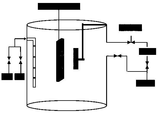
[0025] First, select 5 silicon wafers with a smooth surface, put them into acetone and absolute ethanol in order to ultrasonically clean them for 15 minutes respectively, take out the silicon wafers, blow dry the residual ethanol on the surface of the silicon wafers with nitrogen, and quickly put them into DC reactive magnetron sputtering. On the substrate fixing frame in the vacuum chamber of the injection equipment, keep the substrate surface parallel to the surface of the copper plane target, and keep the distance between the two at 5cm; the sample holder is connected to the negative bias power supply; the copper plane target is connected to the DC power supply. Vacuumize until the vacuum degree is less than 6.0×10 -3 At Pa, pass in argon gas, adjust the air pressure to 2.0Pa, and conduct Ar + Plasma clean for 30 minutes. After the cleaning is completed, a mixed gas of methane and argon is introduced (the flow ratio is 0.7:1), and the DC power supply is turned on. In the c...
Embodiment 2
[0028] First, select 5 silicon wafers with a smooth surface, put them into acetone and absolute ethanol in order to ultrasonically clean them for 15 minutes respectively, take out the silicon wafers, blow dry the residual ethanol on the surface of the silicon wafers with nitrogen, and quickly put them into the vacuum of the physical vapor deposition equipment. On the substrate fixing frame in the cavity, keep the substrate surface parallel to the surface of the nickel plane target, and keep the distance between the two at 10 cm; the sample holder is connected to a negative bias power supply; the nickel plane target is connected to a DC power supply. Vacuumize until the vacuum degree is less than 6.0×10 -3 At Pa, argon gas was introduced, the pressure was adjusted to 0.6 Pa, and Ar+ plasma cleaning was performed for 30 minutes under a DC voltage of 400V bias. After the cleaning is completed, the mixed gas of methane and argon (the flow ratio is 0.2:1) is introduced, the DC powe...
Embodiment 3
[0031] First, select 5 silicon wafers with a smooth surface, put them into acetone and absolute ethanol in order to ultrasonically clean them for 15 minutes respectively, take out the silicon wafers, blow dry the residual ethanol on the surface of the silicon wafers with nitrogen, and quickly put them into the physical vapor deposition equipment. On the substrate fixing frame in the vacuum chamber, keep the substrate surface parallel to the surface of the silver plane target, and keep the distance between the two at 8 cm; the sample holder is connected to a negative bias power supply; the silver plane target is connected to a DC power supply. Vacuumize until the vacuum degree is less than 6.0×10⁻³ At Pa, pass in argon gas, adjust the air pressure to 1.2Pa, and conduct Ar + Plasma clean for 30 minutes. After the cleaning is completed, a mixed gas of methane and argon is introduced (the flow ratio is 0.4:1), the DC power supply is turned on, and the sputtering power of the silve...
PUM
| Property | Measurement | Unit |
|---|---|---|
| hardness | aaaaa | aaaaa |
| thickness | aaaaa | aaaaa |
| thickness | aaaaa | aaaaa |
Abstract
Description
Claims
Application Information

