Assembly of top-emission OLED (Organic Light-Emitting Diode) device and top-emission OLED device

A top-emission and module technology, applied in the field of top-emission OLED components and top-emission OLED devices, can solve the problems of low refractive index matching, sensitivity, and unfavorable light escape of the thin-film packaging layer, so as to achieve tight arrangement and increase transmittance , the effect of chemical stability

Active Publication Date: 2018-10-09
BOE TECH GRP CO LTD
View PDF7 Cites 5 Cited by
  • Summary
  • Abstract
  • Description
  • Claims
  • Application Information

AI Technical Summary

Problems solved by technology

[0005] In the process of realizing the present invention, the inventors have found that the prior art has at least the following problems: the light extraction layer in the prior art usually uses organic small molecule materials that can be evaporated, such as NPB (N, N'-two (1- Naphthyl)-N,N′-diphenyl-1,1′-biphenyl-4-4′-diamine), CBP(4,4′-bis(N-carbazole)-1,1′- Biphenyl), etc., these organic small molecule materials are very sensitive to water vapor and oxygen, and the optical refractive index matching between the light extraction layer and the thin film encapsulation layer above it is low, which is not conducive to light escape. Usually, light passes through the TFE layer The loss is about 8% when

Method used


Image

  • Assembly of top-emission OLED (Organic Light-Emitting Diode) device and top-emission OLED device
  • Assembly of top-emission OLED (Organic Light-Emitting Diode) device and top-emission OLED device
  • Assembly of top-emission OLED (Organic Light-Emitting Diode) device and top-emission OLED device

Examples


preparation example Construction

[0069] Take the preparation process of ZnO as an example: use diethyl zinc and water as the precursors of zinc and oxygen respectively, and pass them into the reactor in turn to form a ZnO film. In each reaction cycle, the exposure time of the precursor was 60 s, and the reaction environment was N 2 , temperature 130°.

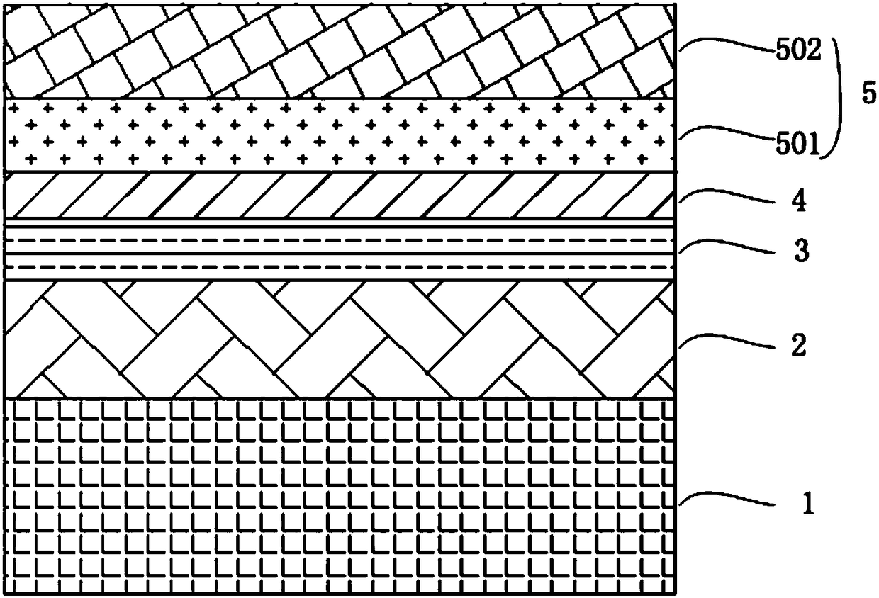
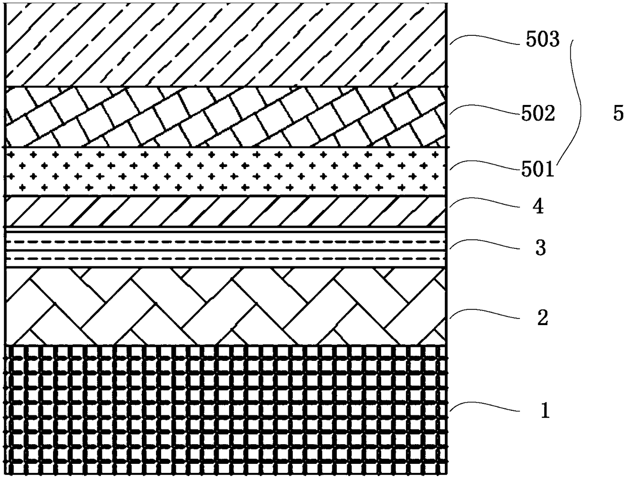
[0070] Furthermore, in the embodiment of the first aspect of the present invention, the material of the first organic encapsulation layer can be epoxy resin; the refractive index of the first organic encapsulation layer is smaller than the refractive index of the light extraction layer, forming a refraction gradient, reducing light total reflection. Further, the thickness of the first organic encapsulation layer may be 1-8 μm, and its refractive index is about 1.56.

[0071] In addition, the material of the first inorganic encapsulation layer can be silicon oxide, silicon nitride or silicon oxynitride, and the refractive index of the first inorganic encapsul...

Embodiment 1

[0094] Put the substrate into acetone, ethanol and deionized water for ten minutes, and then place it in an oven to dry;

[0095] The cleaned substrate is placed in a vacuum chamber, and an anode is formed on the substrate by magnetron sputtering, and the anode is an indium tin oxide / silver / indium tin oxide (ITO / Ag / ITO) film layer;

[0096] Put the prepared substrate into a vacuum evaporation chamber, keep the vacuum at 10-5Pa, use a heating source to heat and sublimate the material, and form a light-emitting layer (hole injection layer / hole injection layer) on the anode by evaporation. transport layer / luminescent layer / electron transport layer / electron injection layer);

[0097]Afterwards, a cathode is formed on the luminescent layer by vacuum evaporation, the thickness of the cathode is 14nm, and the material is a magnesium-silver alloy (the mass ratio of magnesium to silver is 2:8 or 9:1);

[0098] Deposit a light extraction layer on the cathode by atomic layer deposition ...

Embodiment 2

[0103] The difference between embodiment 2 and embodiment 1 lies in the addition of a second organic encapsulation layer. A second organic encapsulation layer with corrugated polymer was formed by layer-by-layer self-assembled polystyrene on the first inorganic encapsulation layer by spin coating.


PUM


Abstract

The invention discloses an assembly of a top-emission OLED (Organic Light-Emitting Diode). The assembly of the top-emission OLED device comprises an anode, a light emitting layer arranged on the anode, a cathode arranged on the light emitting layer, a light extraction layer arranged on the cathode and a packaging layer arranged on the light extraction layer, wherein the light extraction layer is made of a metal oxide, and the packaging layer comprises a first organic packaging layer arranged on the light extraction layer and a first inorganic packaging layer arranged on the first organic packaging layer. The light extraction layer of the assembly of the top-emission OLED device uses the metal oxide which is stable in chemical property and high in refractive index, thereby not only playinga role of isolating water vapor and oxygen to a certain extent for the cathode, the light emitting layer and the anode below, but also improving the transmittance of light through the matching of thelight extraction layer and the packaging layer with the refractive index.

Description

technical field [0001] The invention relates to the technical field of organic electroluminescence display, in particular to a top-emitting OLED component and a top-emitting OLED device. Background technique [0002] Organic Light-Emitting Diode (hereinafter referred to as OLED) devices have the advantages of active light emission, good temperature characteristics, low power consumption, fast response, flexibility, ultra-thin and low cost, and may become a substitute for liquid crystal displays. next-generation display devices. OLED flat panel display technology is tending to the stage of increasingly mature mass production technology and rapid growth of market demand. [0003] OLED devices can be divided into three types according to the direction of light emission: bottom-emitting OLED devices, double-sided emitting OLED devices and top-emitting OLED devices. A bottom-emitting OLED device refers to an OLED device in which light is emitted from a substrate. A double-side...

Claims


Application Information

Patent Timeline
Patent Type & Authority Applications(China)
IPC IPC(8): H01L51/52
CPCH10K50/858H10K50/844H10K2102/3026H10K50/85H10K50/81H10K50/82H10K50/84H10K71/00H10K50/13H10K59/50H10K85/6572
Inventor 王丹
Owner BOE TECH GRP CO LTD
Why Eureka
Try Eureka