Method for preparing Au@InP nanopore array photo-anode plate material

A nanopore array, photoanode technology, applied in anodizing, electrode, electrode shape/type, etc., can solve the problem of easy recombination of photogenerated electrons and holes, and achieve favorable application prospects for diffusion and migration of photogenerated charges. , the effect of high photocurrent density

Inactive Publication Date: 2018-10-12
HUAIBEI NORMAL UNIVERSITY
View PDF0 Cites 1 Cited by
  • Summary
  • Abstract
  • Description
  • Claims
  • Application Information

AI Technical Summary

Problems solved by technology

[0005] In order to solve the deficiencies in the prior art and the problem of easy recombination of photogenerated electrons and holes on the surface of InP nanopores, the purpose of the present invention is to provide a method for preparing Au@InP nanohole array photoanode materials. The synthesized Au@InP On the one hand, the nanohole array photoanode retains the high specific surface area and excellent light absorption characteristics of the nanohole array, and at the same time greatly increases the contact area between Au and InP, which provides great convenience for the separation of photogenerated carriers. , with high photoelectrochemical performance

Method used


Image

  • Method for preparing Au@InP nanopore array photo-anode plate material
  • Method for preparing Au@InP nanopore array photo-anode plate material
  • Method for preparing Au@InP nanopore array photo-anode plate material

Examples


Embodiment 1

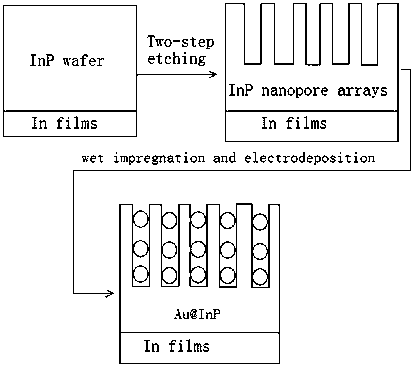
[0037] A method for preparing an Au@InP nanohole array photoanode material. First, an InP wafer is used as a substrate, and a one-dimensional ordered InP nanohole array is prepared by electrochemical anodization combined with wet etching, and then the one-dimensional ordered The InP nanopore array is used as a template, and the Au nanoparticles are uniformly loaded in the InP nanopore array by the impregnation electrochemical deposition method, so as to construct the Au@InP nanopore array composite structure photolysis water photoanode material.

[0038] Such as figure 1 As shown, the preparation of Au@InP nano-heterojunction arrays can be divided into two steps. Firstly, the ordered InP nanohole arrays are prepared by two-step etching method, and then the Au@InP nano-heterojunction arrays are constructed by dipping and electrochemical deposition techniques. Mass knot array.

Embodiment 2

[0040] As a preference of Example 1, the InP wafer is Sn-doped (100) plane n-type single crystal InP, chloroauric acid is the gold source in immersion electrochemical deposition, and neutral sodium chloride solution is the inert electrolyte.

Embodiment 3

[0042] As a preferred embodiment of Example 1, the steps of preparing a one-dimensional InP nanopore array are as follows:

[0043] 1. Perform mechanical mirror polishing on one side of the InP wafer, clean the polished InP wafer to remove the oil on the surface of the InP wafer, then rinse the InP wafer with deionized water several times, and then dry it for later use;

[0044] 2. Use DC magnetron sputtering method to sputter indium film on the unpolished surface of the InP wafer obtained in step 1, and then anneal at a certain temperature. After the annealing, cut the InP wafer into samples of the same size, and then use high-purity The conductive silver paste connects one side of the indium-plated film of the InP sample to the copper wire to prepare the InP electrode;

[0045] 3. Use the InP electrode in step 2 as the anode, and the graphite sheet as the cathode, put the anode and the cathode into the hydrochloric acid solution, and connect the stabilized power supply betwe...


PUM

PropertyMeasurementUnit
particle diameteraaaaaaaaaa

Abstract

The invention discloses a method for preparing an Au@InP nanopore array photo-anode plate material. The method comprises the steps that firstly, an InP wafer is adopted as a substrate, and a one-dimensional ordered InP nanopore array through an anodic oxidation method in combination with wet etching; and then the one-dimensional ordered InP nanopore array is adopted as a template, the InP nanoporearray is evenly loaded with Au nano particles through a dipping electrochemical deposition method, and therefore the Au@InP nanopore array complex structure photoelectrolysis water photo-anode platematerial is constructed. According to the Au@InP nanopore array complex structure, the contact area of a heterojunction can be greatly increased, and meanwhile reactivity sties can be greatly increased. High light current density, low take-off potential and excellent photon-generated carrier separation capability are achieved. Operation is flexible and easy, the reaction conditions are mild, and cost is low. Obtained Au nano particles are good in size uniformity, easy to regulate and control and suitable for large-scale production and has good application prospects.

Description

technical field [0001] The invention relates to a preparation method of a photoanode material for hydrogen production by photolysis of water, in particular to a preparation method of an Au@InP nanohole array photoanode material. Background technique [0002] Since Japanese scientists reported TiO in 1972 2 Since the photoelectric splitting of water by electrodes, hydrogen production from photoelectrochemical water splitting has attracted extensive attention. In the photoelectrochemical water splitting reaction, the oxygen evolution reaction on the photoanode is thermodynamically or kinetically more difficult than the hydrogen evolution reaction on the photocathode, and it is the bottleneck of the energy conversion efficiency of the entire water splitting system. Therefore, the development of efficient and stable water-splitting photoanode materials has received widespread attention from scientists at home and abroad. [0003] At present, the most commonly used photoanode m...

Claims


Application Information

Patent Timeline
Patent Type & Authority Applications(China)
IPC IPC(8): C25B1/04C25B11/03C25B11/04C25D11/02C25D3/48C25D5/54
CPCC25B1/04C25B11/03C25B11/04C25D3/48C25D5/54C25D11/02C25B1/55Y02E60/36
Inventor 李强代凯张金锋李宏朱光平张敏
Owner HUAIBEI NORMAL UNIVERSITY
Why Eureka
Try Eureka