Organic-inorganic composite perovskite light-emitting diode device and fabrication method thereof
A light-emitting diode and perovskite technology, which is applied in the field of organic-inorganic composite perovskite light-emitting diode devices and its preparation, can solve the problems of low luminous efficiency and external quantum efficiency of perovskite light-emitting diodes, and achieve improved photoelectric conversion efficiency effect
- Summary
- Abstract
- Description
- Claims
- Application Information
AI Technical Summary
Problems solved by technology
Method used
Image

Examples
Embodiment 1
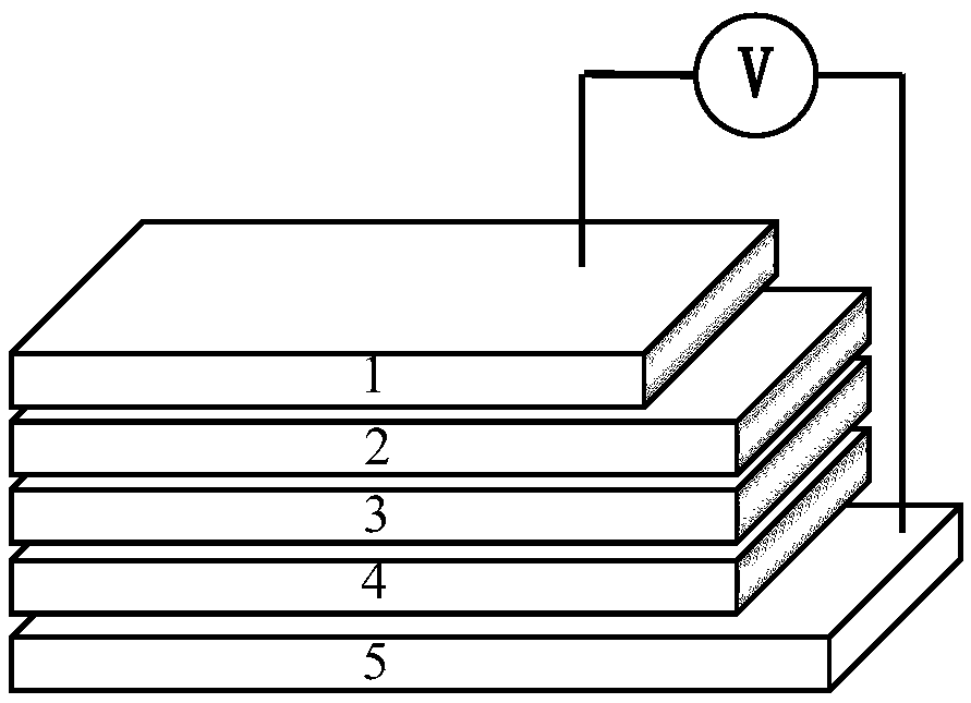
[0035] see figure 1 , the FA-MA organic-inorganic composite perovskite light-emitting diode device of the present invention, from bottom to top, is a transparent conductive anode ITO, a hole injection layer, a hole transport layer, an organic-inorganic perovskite light-emitting layer, and an electron transport layer. , metal conductive electrodes. Each layer is described in detail below.
[0036] Among them, the transparent conductive anode layer is made of inorganic material, indium tin oxide (ITO), with a thickness of about 200nm;
[0037] The hole injection layer of the present invention adopts PEDOT:PSS (poly 3,4-ethylenedioxythiophene / polystyrene sulfonate), which is characterized in that the injection layer will be used to improve the work function of the conductive anode ITO, which is more conducive to the formation of holes. injection;
[0038] The hole transport layer of the present invention is TFB (poly (9,9-dioctyl fluorene-CO-N-(4-butylphenyl) diphenylamine); t...
preparation example
[0043] For FA 1-x MA x PbBr 3 Example method for the preparation of perovskite nanocrystals:
[0044] Step 1, hydrobromic acid (HBr) and methylamine (CH 3 NH 2 ) was stirred for two hours in an ice bath, and after the two fully reacted, dried at 60°C to obtain the reactant, then washed the reactant three times with ether and dried in vacuum for 24 hours to obtain a white fluffy powder, and obtained methyl Ammonium bromide (MABr);
[0045] Step 2, 0.8mmol of FABr and MABr in different molar ratios (9:1 and 8:2) were dissolved in 0.5ml DMF respectively to prepare solution A;
[0046] Step 3, 1mmol PbBr 2 Dissolve in 0.5ml DMF to make solution B;
[0047] Step 4, drop an appropriate amount of oleic acid (OA) and oleylamine (OLA) into the mixed liquid of solutions A and B, and stir until the mixed solution becomes transparent to obtain solution C;
[0048] Step 5, slowly drop solution C into 10ml of toluene, and stir until the solution becomes clear green, then add 5ml of ...
Embodiment 3
[0054] based on figure 1 The structural schematic diagram of the organic-inorganic composite type perovskite light-emitting diode shown, the present invention provides a kind of preparation method of the perovskite light-emitting diode of embodiment, this method comprises the following steps:
[0055] 1) Etch the ITO glass into a narrow band with a laser marking machine, and ultrasonically clean it with acetone, isopropanol, and deionized water for 20 minutes, and use the ITO glass as the transparent anode layer of the device. The square resistance of the ITO glass is about 15 ~30Ω, the thickness is about 200nm;
[0056] 2) Preparation of the hole injection layer: Treat the ITO glass treated in step 1) with ozone for 30 minutes using a UV cleaning machine, then spin-coat PEDOT:PSS on the transparent anode layer ITO glass at a speed of 5000rpm / min, and spin Coat 4 layers, PEDOT:PSS film thickness is about 220~240nm; then anneal at 150°C for 30 minutes;
[0057] 3) Preparation...
PUM
| Property | Measurement | Unit |
|---|---|---|
| Thickness | aaaaa | aaaaa |
| Thickness | aaaaa | aaaaa |
| Thickness | aaaaa | aaaaa |
Abstract
Description
Claims
Application Information
 - Generate Ideas
- Intellectual Property
- Life Sciences
- Materials
- Tech Scout
- Unparalleled Data Quality
- Higher Quality Content
- 60% Fewer Hallucinations
Browse by: Latest US Patents, China's latest patents, Technical Efficacy Thesaurus, Application Domain, Technology Topic, Popular Technical Reports.
© 2025 PatSnap. All rights reserved.Legal|Privacy policy|Modern Slavery Act Transparency Statement|Sitemap|About US| Contact US: help@patsnap.com