

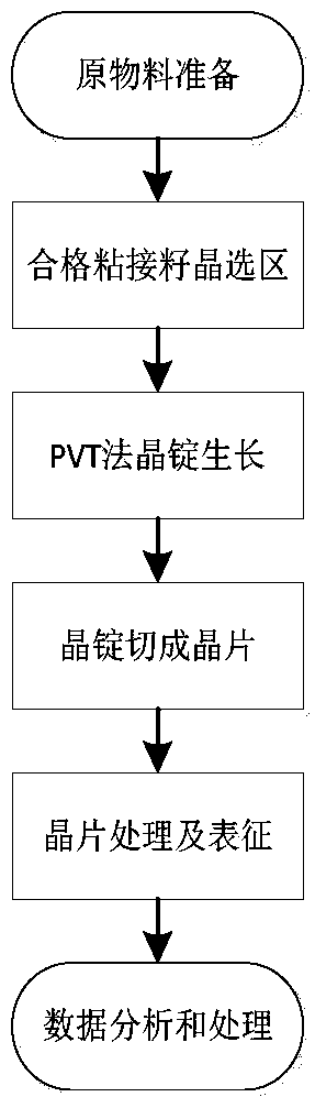
Bonding method of silicon carbide seed crystals and preparation method of silicon carbide single-crystal ingot
A silicon carbide seed and bonding method technology is applied to the preparation of silicon carbide single crystal ingots and the bonding field of silicon carbide seed crystals. Improve the growth quality and pass rate, solve the temperature unevenness, and ensure the effect of temperature uniformity
- Summary
- Abstract
- Description
- Claims
- Application Information
AI Technical Summary
Problems solved by technology
Method used
Image

Examples
Embodiment 1
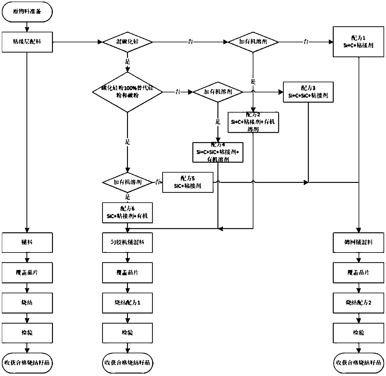
[0040] A method for bonding silicon carbide seed crystals, comprising the following steps:
[0041] (1) Mix silicon powder, carbon powder and silicon carbide powder, add starch as a binder, and ethylene glycol as an organic solvent, mix with a mixer at a speed of 2000 rpm for 1 hour, and obtain a mixed material with uniform color; wherein the silicon powder The mass ratio to carbon powder is 7:3; silicon carbide powder accounts for 5% of the total mass of silicon powder and carbon powder; starch accounts for 5% of the total mass of silicon powder and carbon powder;
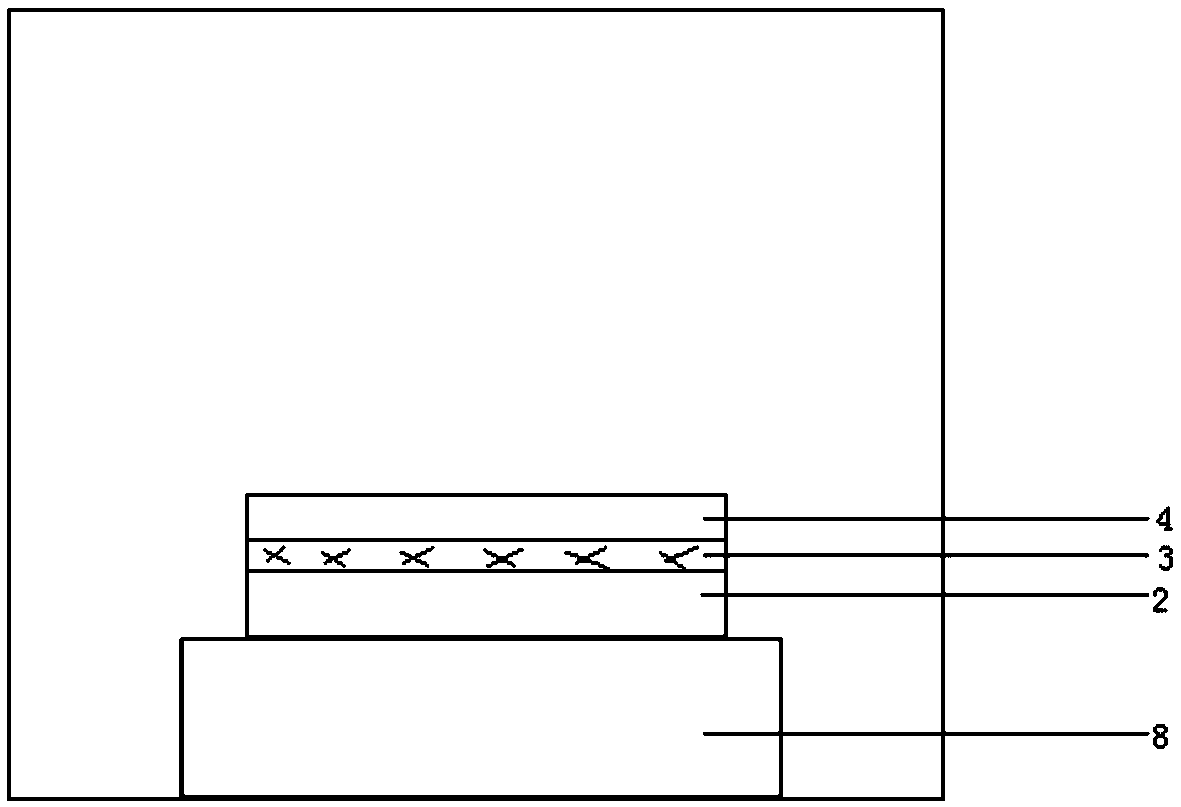
[0042] (2) Spread the mixed material evenly on a silicon carbide wafer with a thickness of 300 μm with a homogenizer;
[0043] (3) placing the silicon carbide seed crystal on the mixed material on the silicon carbide wafer;
[0044] (4) Put the silicon carbide wafer in the step (3) into the heating furnace, such as image 3 As shown, under the protection of inert gas, according to the heating rate of 1000 ℃ / h,...
Embodiment 2
[0047] A method for bonding silicon carbide seed crystals, comprising the following steps:
[0048] (1) Mix silicon powder, carbon powder and silicon carbide powder, add dextrin as a binder, and mix with a mixer at a speed of 2000rpm for 1 hour to obtain a mixed powder with uniform color; wherein the mass ratio of silicon powder to carbon powder is 7:3; silicon carbide powder accounts for 10% of the total mass of silicon powder and carbon powder; dextrin accounts for 5% of the total mass of silicon powder and carbon powder;
[0049] (2) Hand-sprinkle the mixed powder evenly with a sieve on a silicon carbide wafer with a thickness of 300 μm;
[0050] (3) placing the silicon carbide seed crystal on the mixed powder on the silicon carbide wafer;
[0051] (4) Put the silicon carbide wafer in step (3) into a heating furnace, and heat it at 1700°C for 8 hours under the protection of an inert gas, and then the silicon carbide seed crystal and the silicon carbide wafer can be bonded ...
Embodiment 3
[0054] A method for bonding silicon carbide seed crystals, comprising the following steps:
[0055] (1) Mix the silicon carbide powder and starch with a mixer at a speed of 3000 rpm for 1 hour to obtain a mixed powder with uniform color; wherein the starch accounts for 8% of the mass of the silicon carbide powder;
[0056] (2) Hand-sprinkle the mixed powder evenly with a sieve on a silicon carbide wafer with a thickness of 300 μm;
[0057] (3) placing the silicon carbide seed crystal on the mixed powder on the silicon carbide wafer;
[0058] (4) Put the silicon carbide wafer in step (3) into a heating furnace, and heat it at 1800°C for 9 hours under the protection of an inert gas, and then the silicon carbide seed crystal and the silicon carbide wafer can be bonded tightly to obtain bonded carbonization Silicon seed. The samples in this step are subjected to double-sided visual inspection, strong light transmission visual inspection on the back, surface inspection on an opti...
PUM
| Property | Measurement | Unit |
|---|---|---|
| thickness | aaaaa | aaaaa |
| particle diameter | aaaaa | aaaaa |
| thickness | aaaaa | aaaaa |
Abstract
Description
Claims
Application Information