Preparation method and application of two-dimensional lead telluride nano sheet and nano material

A nanomaterial, lead telluride technology, applied in the field of nanomaterials, can solve the problems of limiting the application of PbTe, poor process compatibility, high price, etc., and achieve the effects of good optoelectronic performance, low production equipment cost, and low price.

Active Publication Date: 2019-04-19
SUZHOU INST OF NANO TECH & NANO BIONICS CHINESE ACEDEMY OF SCI
View PDF8 Cites 11 Cited by
  • Summary
  • Abstract
  • Description
  • Claims
  • Application Information

AI Technical Summary

Problems solved by technology

[0005] In addition, traditional PbTe thin film preparation processes mainly include chemical bath deposition, molecular beam epitaxy, vacuum evaporation deposition and other technologies, but the above preparation processes have disadvantages such as high price, thicker films, and poor compatibility with microelectronic device processes (Wu H F ,Chen Yao,et al.Molecular Beam Epitaxy Growth and Surface StructuralCharacteristics of PbTe(111)Thin Film[J].Acta Phys.-Chim.Sin.2017,33(2),419-425), these unfavorable factors limit Application of PbTe in Infrared Optoelectronics

Method used


Image

  • Preparation method and application of two-dimensional lead telluride nano sheet and nano material
  • Preparation method and application of two-dimensional lead telluride nano sheet and nano material
  • Preparation method and application of two-dimensional lead telluride nano sheet and nano material

Examples


preparation example Construction

[0040] The following introduces the preparation method of the two-dimensional lead telluride nanosheet based on the above-mentioned growth system of the present invention, including:

[0041] 1) Weighing the reaction raw materials used for the growth of two-dimensional lead telluride nanosheets;

[0042] 2) Using sheet-like materials with atomic-level smooth surfaces as growth substrates;

[0043] 3) In the air flow of the protective gas, after the temperature is programmed, the reaction raw materials are heated at a constant temperature to perform vapor deposition;

[0044] 4) quenching the substrate after the deposition process is completed, that is, obtaining the two-dimensional lead telluride nanosheets on the substrate;

[0045] Specifically, the reaction raw materials include, but are not limited to, lead telluride powder, lead telluride block, tellurium simple substance, tellurium-containing compound, lead simple substance and / or lead-containing compound.

[0046] It ...

Embodiment 1

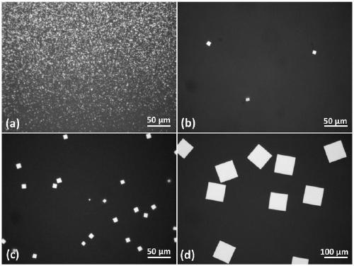
[0087] This embodiment discloses a method for preparing two-dimensional lead telluride nanosheets, which specifically includes:

[0088] (1) Preparation of mica sheet substrate

[0089] a) the mica sheet is divided into squares of 1.5cm*1.5cm;

[0090] b) Use a blade or scissors to dissociate the mica sheet from the middle into 3 to 4 pieces, and use the newly dissociated smooth plane as the growth surface.

[0091] (2) Weigh 400mg of PbTe powder, put it in a quartz boat, then connect the quartz boat with the magnet in the furnace with an iron wire, and put it into the upstream of the gas path of the horizontal tube furnace, specifically 40-50cm away from the heating center Use the magnet outside the furnace tube of the tube furnace to attract the magnet in the furnace; place the mica sheet in the downstream of the gas path of the horizontal tube furnace, specifically at a position 5-25cm away from the heating center;

[0092] (3) Utilize the vacuum pump to evacuate the hori...

Embodiment 2

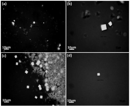
[0103] This embodiment discloses a method for preparing two-dimensional lead telluride nanosheets, which specifically includes:

[0104] (1) Preparation of fluorine phlogopite sheet substrate

[0105] a) Divide the fluorphlogopite sheet into squares of 1.5cm*1.5cm;

[0106] b) Use a blade or scissors to peel off the fluorophlogopite sheet along the (001) surface into 3-4 pieces, and use the newly dissociated smooth plane as the growth surface.

[0107] (2) Weigh 400mg of PbTe powder, put it in a quartz boat, then connect the quartz boat with the magnet in the furnace with an iron wire, and put it into the upstream of the gas path of the horizontal tube furnace, specifically 40-50cm away from the heating center Place the fluorophlogopite sheet in the downstream of the gas path of the horizontal tube furnace, specifically at a position 5-25cm away from the heating center;

[0108] (3) Utilize the vacuum pump to evacuate the horizontal tube furnace. When the pressure in the fur...


PUM

PropertyMeasurementUnit
thicknessaaaaaaaaaa
electron mobilityaaaaaaaaaa
thicknessaaaaaaaaaa

Abstract

The invention relates to the technical field of nano materials, in particular to a preparation method and application of a two-dimensional lead telluride nano sheet and a nano material. The method comprises the steps that a reaction raw material which is used for the growing of the lead telluride nano sheet is weighed; a sheet-like material with a surface with an atomic level smoothness is taken as a growing substrate; the reaction raw material is thermostatically heated to perform vapor deposition in a protective gas flow after programmed temperature increasing; the substrate is allowed to bequenched after the decomposition process is completed, and the two-dimensional lead telluride nano sheet is obtained on the substrate. The thickness of the nano sheet is 5 nm-200 nm, the width or length is 0.1-70 microns, and the nano sheet is provided with a monocrystalline structure. The nano sheet is of a face-centered cubic crystal, and the exposed crystal face of the nano sheet belongs to {100} crystal face family and is provided with a sheet-like rectangular morphology; the ultra-thin two-dimensional lead telluride nano sheet with large area, uniform orientation and morphology and crystallinity can be obtained through a Van der waals epitaxy technology, and the two-dimensional lead telluride nano sheet can be applied to the fields of infrared ray photoelectric detectors and the like.

Description

technical field [0001] The invention relates to the technical field of nanomaterials, in particular to a preparation method and application of a two-dimensional lead telluride nanosheet and a nanomaterial. Background technique [0002] Since the discovery of graphene by Novoselov et al. in 2004, two-dimensional materials have received widespread attention. As the first generation of two-dimensional materials, graphene exhibits excellent properties. For example, the strength of graphene can reach 130GPa (Lee C, WeiX, Kysar J W, et al.Measurement of the elastic properties and intrinsic strength of monolayer[J].Science,2008,321(5887),385), the electron mobility at room temperature is as high as 15000cm 2 / (V·s) et al. (Geim A K, Novoselov K S. The rise of graphene [J]. Nat Mater, 2007, 6(3), 183). However, graphene lacks a band gap, has poor light absorption ability, and has a low on-off ratio. It cannot realize the logic switch of semiconductors, and it is difficult to apply ...

Claims


Application Information

Patent Timeline
Patent Type & Authority Applications(China)
IPC IPC(8): C01B19/04B82Y40/00H01L31/032H01L29/24
CPCH01L29/245H01L31/0322B82Y40/00C01B19/007C01P2002/85C01P2004/02C01P2004/04C01P2004/03C01P2002/82C01P2004/20Y02E10/541
Inventor 张凯阴晴
Owner SUZHOU INST OF NANO TECH & NANO BIONICS CHINESE ACEDEMY OF SCI
Why Eureka
Try Eureka