
A near-infrared photoelectric device and a processing method thereof

A near-infrared light and processing method technology, applied in optical components, metal processing equipment, metal processing mechanical parts, etc., can solve the problems of weak photoelectric response ability, slow device response speed, etc., to achieve short response time, uniform gap size, The effect of improving optical and electrical performance

Active Publication Date: 2019-05-10
HARBIN INST OF TECH
View PDF5 Cites 0 Cited by
  • Summary
  • Abstract
  • Description
  • Claims
  • Application Information

AI Technical Summary

Problems solved by technology

At present, there are still deficiencies in the research of near-infrared wavelength-responsive optoelectronic devices based on nanomaterials, such as slow response speed of devices and weak photoelectric response capabilities.

Method used


Image

  • A near-infrared photoelectric device and a processing method thereof
  • A near-infrared photoelectric device and a processing method thereof
  • A near-infrared photoelectric device and a processing method thereof

Examples


Embodiment 1

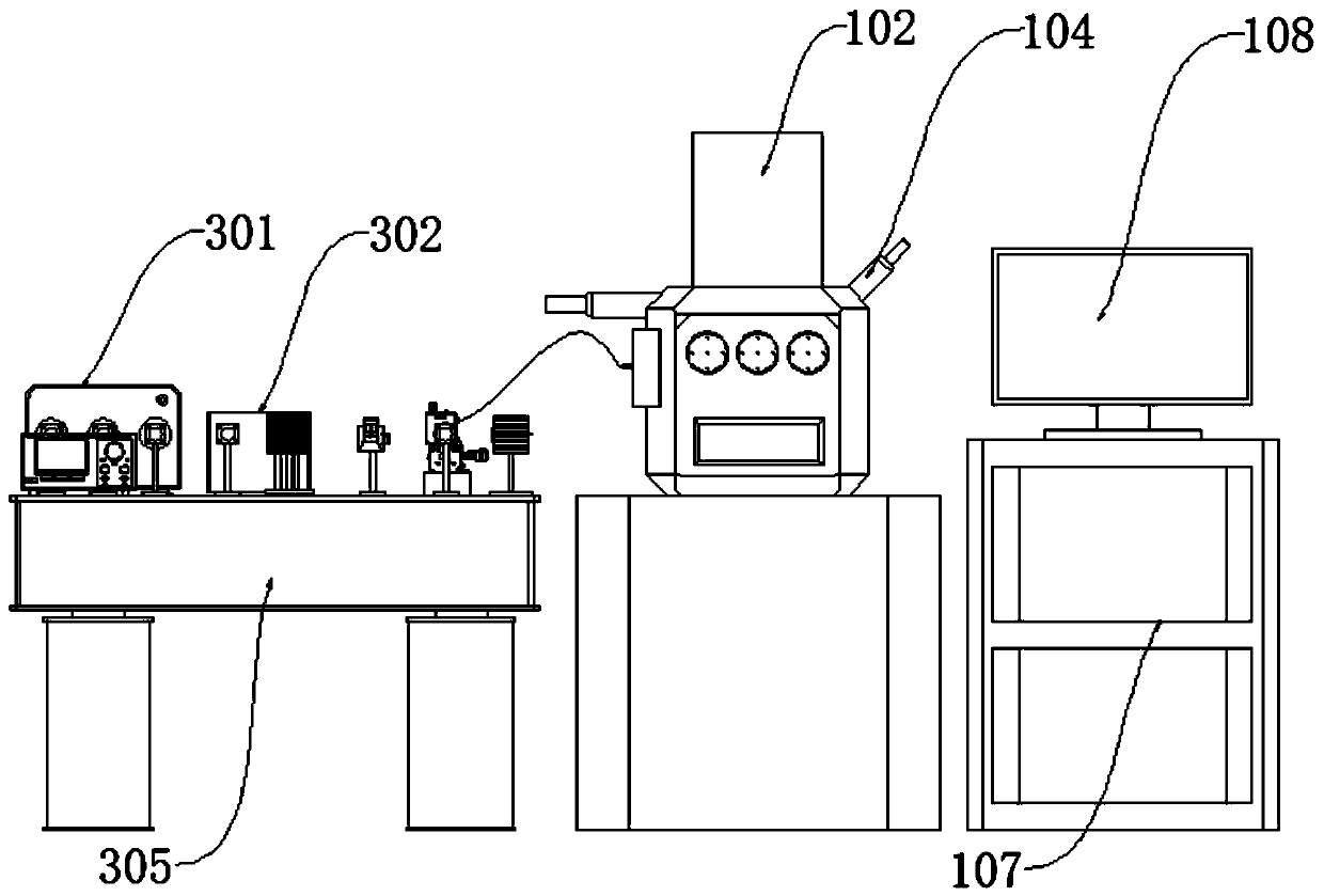
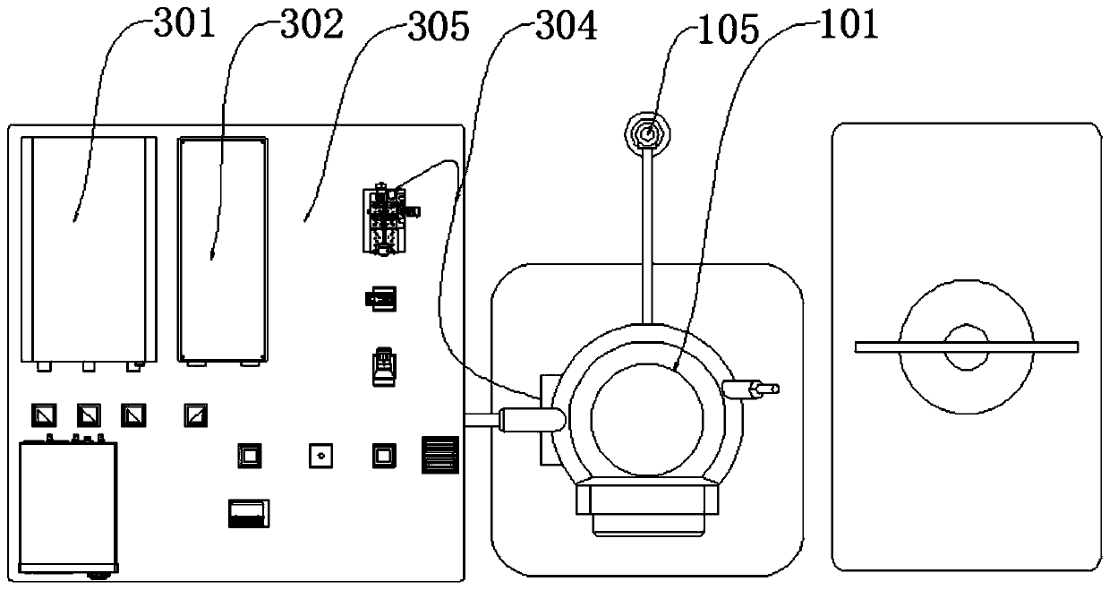
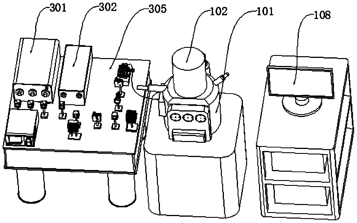
[0070] A nano-junction device, such as Figure 1 to Figure 3 As shown, it includes a vacuum cavity 101, a near-field light generating device, a nano-manipulation device and a control device 107, the near-field light generating device includes a vacuum cavity laser emitting device and an execution end, and the nano-manipulation device includes a sample stage and an execution end Operating device; the nano-manipulating device is arranged inside the vacuum chamber 101, the execution end is connected to the execution-end operating device, the near-field light generating device and the nano-manipulating device are respectively connected to the control device 107 connected; the sample stage is suitable for moving the sample, and the execution end operation device is suitable for driving the execution end to move.

[0071] Here, the sample is a silicon wafer with nanoparticles and nanowires dispersed on its surface. In actual operation, the sample stage is provided with a sample plac...

Embodiment 2

[0074] Like the embodiment described above, this embodiment differs from it in that, as Figure 1 to Figure 4 As shown, the near-field light generating device includes: a laser emitting device, a fiber coupler 303 and an execution end, the laser emitting device is suitable for generating a laser beam, and the fiber coupler 303 is connected to the execution end through an optical fiber 304, so The fiber coupler 303 is suitable for coupling the laser beam into the optical fiber 304; the execution end is suitable for generating near-field light by using the laser beam.

[0075] The advantage of this arrangement is that the spatially free laser beam is coupled into the optical fiber 304 through the optical fiber coupler 303 , and then the optical fiber 304 is used to connect to the execution end, and the laser beam is delivered to the execution end through the optical fiber 304 .

[0076] Such as Figure 1 to Figure 4 As shown, the laser emitting device and the fiber coupler 303 ...

Embodiment 3

[0080] Like the embodiment described above, this embodiment differs from it in that, as Figure 1 to Figure 4 As shown, the laser emitting device includes a laser 301 and a laser parameter amplifier 302, the laser 301 is suitable for emitting the laser beam, the laser beam is emitted through the laser 301, and then enters the laser parameter amplifier 302, so The laser parameter amplifier 302 is suitable for adjusting the wavelength of the laser beam. The advantage of such setting is that the wavelength of the laser beam can be controlled through the setting of the laser parameter amplifier 302 .

[0081] Optionally, as in image 3 and Figure 4 As shown, the laser emitting device also includes a reflector 313, the mirror surface 315 of the reflector 313 presents a set angle with the laser beam emitted by the laser 301, and the reflector 301 is suitable for the The laser beam emitted by the laser 301 is reflected to the laser parameter amplifier 302 . The advantage of this...


PUM

PropertyMeasurementUnit
diameteraaaaaaaaaa
porosityaaaaaaaaaa
diameteraaaaaaaaaa

Abstract

The invention provides a near-infrared photoelectric device and a processing method thereof, and relates to the technical field of processing and manufacturing. The near-infrared photoelectric deviceincludes a silicon substrate, a number of nano optical antennas, two electrodes and a nano wire, wherein the nano optical antennas and the two electrodes are arranged on the surface of the silicon substrate, all the nano optical antennas are located between the two electrodes, the two ends of the nano wire are connected with the two electrodes respectively, and the nano wire is in contact with atleast one nano optical antenna. The invention further provides a processing method of the near-infrared photoelectric device. When the gap between the large disc and the small disc in the same nanometer optical antenna is illuminated, plasmon can be excited, incident light can be captured and enhanced, the response wavelength range of the device is widened, the carrier concentration in the nanowire is improved, and then the optical and electrical properties of the device are improved.

Description

technical field [0001] The invention relates to the technical field of processing and manufacturing, in particular to a near-infrared optoelectronic device and a processing method thereof. Background technique [0002] With the increasingly higher requirements for the integration of chips and electronic devices in various fields, the feature size of electronic devices is continuously reduced. However, traditional electronic devices based on semiconductor materials such as silicon will face huge challenges: on the one hand, according to predictions, the feature size of traditional electronic devices will stop reducing in the future; on the other hand, as feature sizes enter the nanometer level, traditional There are problems such as thermal effect and size effect in electronic devices, which seriously affect the performance and application of electronic devices. In recent years, due to their excellent mechanical, electrical and optical properties, nanomaterials are considere...

Claims


Application Information

Patent Timeline
Patent Type & Authority Applications(China)
IPC IPC(8): B81C3/00B81B7/04B81C99/00
Inventor 王扬侯超剑杨立军王根旺丁烨赵春洋
Owner HARBIN INST OF TECH
Learn More