Preparation method of ZnO modified WO3/BiVO4 heterojunction as well as application of ZnO modified WO3/BiVO4 heterojunction to photoelectrocatalysis
A heterojunction, composite light technology, applied in physical/chemical process catalysts, metal/metal oxide/metal hydroxide catalysts, chemical instruments and methods, etc., can solve the problem of short lifetime of photogenerated carriers and weak visible light response , low photon absorption coefficient, etc., to achieve the effects of improving photoelectric catalytic performance, accurate and controllable deposition thickness, and simple and controllable process
- Summary
- Abstract
- Description
- Claims
- Application Information
AI Technical Summary
Problems solved by technology
Method used
Image

Examples
Embodiment 1
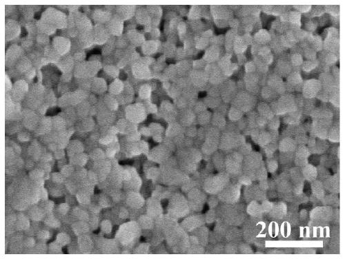
[0046] Weigh 0.1g PVP and 2g WCl respectively 6 Dissolved in 10 mL DMF, and stirred at room temperature for 1 hour to obtain a spin coating solution. Take 20μL spin-coated on the conductive surface of FTO glass at a speed of 4000 rpm, dry at 80°C for 3 hours, and anneal in a muffle furnace at 500°C for 1 hour to form WO 3 Seed layer. figure 1 For the obtained WO 3 The scanning electron microscope (SEM) picture of the seed layer, it can be seen that it is composed of extremely small WO 3 It is composed of particles and densely covers the conductive surface of FTO.
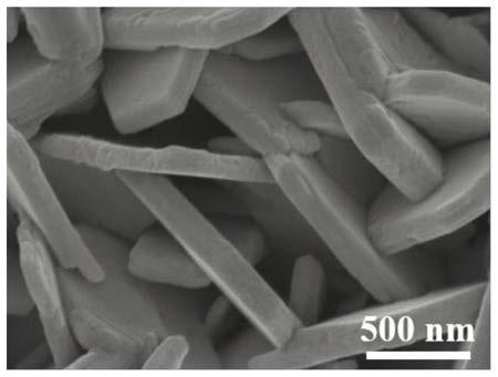
[0047] 0.25g Na 2 WO 4 Dissolve in 30mL of water, add 6mL of 3M HCl, stir evenly, then add 0.2g (NH 4 ) 2 C 2 O 4 , Add water to 70mL and stir until a clear solution is formed. Take 28mL of the above-prepared solution, add and place WO 3 In the FTO reactor of the seed layer, react at 120°C for 12 hours. After the reaction is finished and cooled, the electrode surface is cleaned with deionized water and ethanol, and the...
Embodiment 2
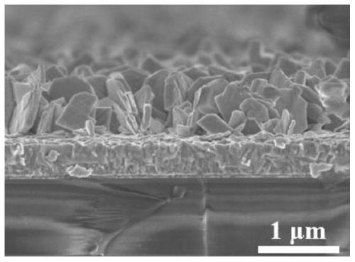
[0052] The only difference from Embodiment 1 is that the deposition cycle of the ZnO layer is 30 times. The other processes are the same as Embodiment 1, and will not be repeated here. The cross-sectional scanning electron microscope (SEM) of the prepared photoelectrocatalytic anode material is as Picture 10 As shown, the surface morphology has not changed significantly, indicating that the ZnO layer is extremely thin.
Embodiment 3
[0054] The only difference from Embodiment 1 is that the deposition cycle of the ZnO layer is 100 times. The other processes are the same as Embodiment 1, and will not be repeated here. The cross-sectional scanning electron microscope (SEM) of the prepared photoelectrocatalytic anode material is as Picture 11 As shown, the surface morphology has not changed significantly.
PUM
 Abstract
Description
Claims
Application Information
 - R&D
- Intellectual Property
- Life Sciences
- Materials
- Tech Scout
- Unparalleled Data Quality
- Higher Quality Content
- 60% Fewer Hallucinations
Browse by: Latest US Patents, China's latest patents, Technical Efficacy Thesaurus, Application Domain, Technology Topic, Popular Technical Reports.
© 2025 PatSnap. All rights reserved.Legal|Privacy policy|Modern Slavery Act Transparency Statement|Sitemap|About US| Contact US: help@patsnap.com