Laser processing method for improving TCO thin film comprehensive optical and electrical properties
A laser processing method and technology of optoelectronic characteristics, applied in the direction of copying/marking method, circuit, electrical components, etc., can solve the problems of conductivity damage, difficult to control corrosion speed and thickness, high sensitivity, improve conductivity and facilitate promotion , a wide range of effects
- Summary
- Abstract
- Description
- Claims
- Application Information
AI Technical Summary
Problems solved by technology
Method used
Image

Examples
Embodiment 1
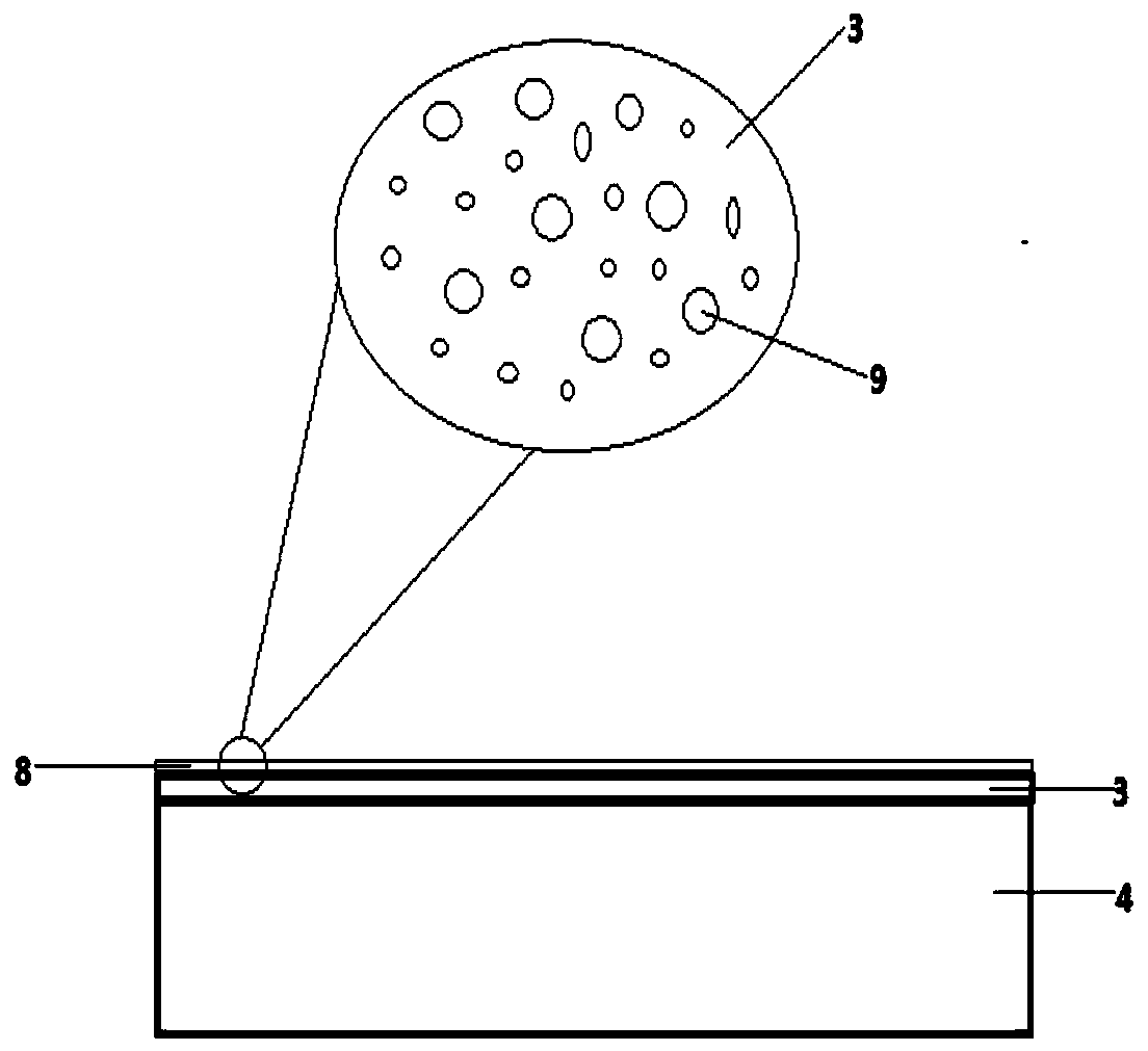
[0030] In this embodiment, the metal material is selected as silver (Ag), and the TCO film is selected as an aluminum-doped zinc oxide (AZO) film, and the photoelectric performance is improved by doping Ag particles on the surface of the AZO film;
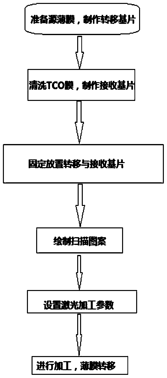
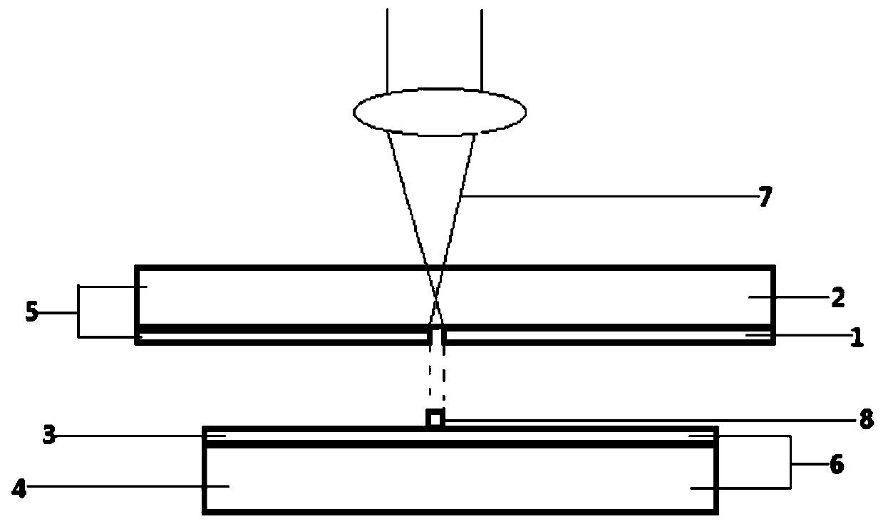
[0031] Step 1, the metal Ag to be doped is deposited on the surface of the transfer substrate 2 by vacuum magnetron sputtering. At this time, the metal Ag exists in the form of a film and serves as the source film 1, and the thickness of the film is controlled to 50nm by controlling the sputtering time , the quality of the source film formed in this way is better, and its size is 20×20mm. The source film 1 and the transfer substrate 2 are collectively referred to as the transfer substrate 5;
[0032] Step 2, select AZO to be prepared on the receiving substrate 4, wash it, dry it and use it as the receiving substrate 6; the size of the AZO glass is 15×15×2mm, the transmittance of visible light is 80%, and the square resistance is 9.5...
Embodiment 2
[0041] Silver (Ag) is selected as the metal material, and fluorine-doped tin dioxide (FTO) film is selected as the TCO film, and the photoelectric performance is improved by doping Ag particles on the surface of the FTO film;
[0042] Step 1, the metal Ag to be doped is deposited on the surface of the transfer substrate 2 by vacuum magnetron sputtering. At this time, the metal Ag exists in the form of a film and serves as the source film 1, and the thickness of the film is controlled to 30nm by controlling the sputtering time , the quality of the source film formed in this way is better, and its size is 20×15 mm. The source film 1 and the transfer substrate 2 are collectively referred to as the transfer substrate 5;
[0043] Step 2, select the FTO film to be prepared on the receiving substrate 4, wash it, dry it for standby, and use it as the receiving substrate 6; the size of the FTO film glass is 10×10×1mm, the visible light transmittance is 78.02%, and the square resistance ...
Embodiment 3
[0053] Silver (Ag) is selected as the metal material, aluminum-doped zinc oxide (AZO) film is selected as the TCO film, and the photoelectric performance is improved by doping Ag particles on the surface of the AZO film.
[0054] Step 1, the metal Ag to be doped is deposited on the surface of the transfer substrate 2 by vacuum magnetron sputtering. At this time, the metal Ag exists in the form of a film and serves as the source film 1, and the thickness of the film is controlled to be 100nm by controlling the sputtering time , the quality of the source film formed in this way is better, and its size is 20×20mm. The source film 1 and the transfer substrate 2 are collectively referred to as the transfer substrate 5;
[0055] Step 2, select the AZO film to be prepared on the receiving substrate 4, wash it, dry it and use it as the receiving substrate 6; the size of the AZO glass is 15×15×2mm, the transmittance of visible light is 79.46%, and the square resistance is 9.39Ω / sq, th...
PUM
| Property | Measurement | Unit |
|---|---|---|
| Sheet resistance | aaaaa | aaaaa |
| Sheet resistance | aaaaa | aaaaa |
| Sheet resistance | aaaaa | aaaaa |
Abstract
Description
Claims
Application Information
 - Generate Ideas
- Intellectual Property
- Life Sciences
- Materials
- Tech Scout
- Unparalleled Data Quality
- Higher Quality Content
- 60% Fewer Hallucinations
Browse by: Latest US Patents, China's latest patents, Technical Efficacy Thesaurus, Application Domain, Technology Topic, Popular Technical Reports.
© 2025 PatSnap. All rights reserved.Legal|Privacy policy|Modern Slavery Act Transparency Statement|Sitemap|About US| Contact US: help@patsnap.com