Preparation method of HCl gas sensor based on two-dimensional Au@MOFs nanoparticle ordered array
A nanoparticle array and gas sensor technology, which is applied in the direction of instruments, scientific instruments, phase influence characteristic measurement, etc., can solve the problems of low response sensitivity, poor selectivity, PS nanospheres and substrate falling off, etc., and achieve high selectivity detection, Good sensitivity, not easy to fall off
- Summary
- Abstract
- Description
- Claims
- Application Information
AI Technical Summary
Problems solved by technology
Method used
Image
Examples
preparation example Construction
[0028] The prepared quartz-based two-dimensional Au nanoparticle array comprises:
[0029] Using the two-dimensional polymer microsphere array on the quartz substrate as a template, it is prepared by depositing an Au layer and annealing at a high temperature of 900-1000°C for 2 hours.
[0030] The physical deposition methods include magnetron sputtering deposition, thermal evaporation deposition or electron beam evaporation deposition.
[0031] The thermal decomposition and annealing treatment of the above-mentioned template deposited with gold film includes:
[0032] Put the above-mentioned template deposited with gold film into a tube furnace, and heat and anneal at 900-1000°C in an air atmosphere for 2 hours. The single-layer polymer colloidal crystal array on the quartz base is thermally decomposed, while the Au film on the quartz base It will melt, fuse, and solidify in situ to form a periodic quartz-based two-dimensional Au nanoparticle array.
[0033] The preparation ...
Embodiment 1
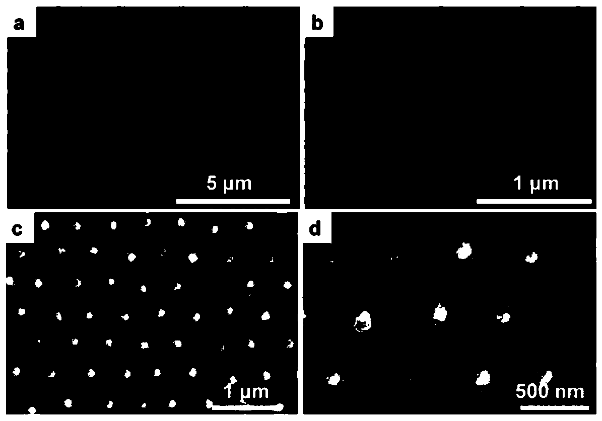
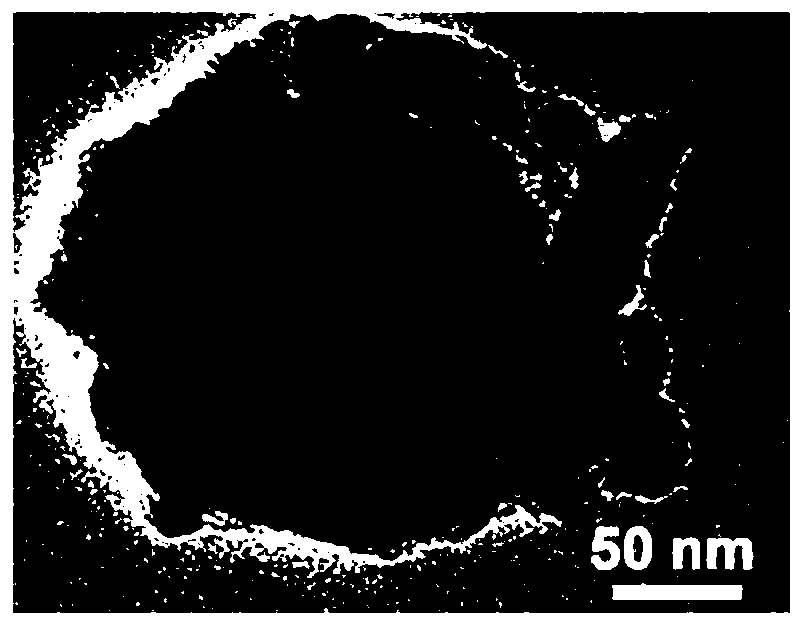
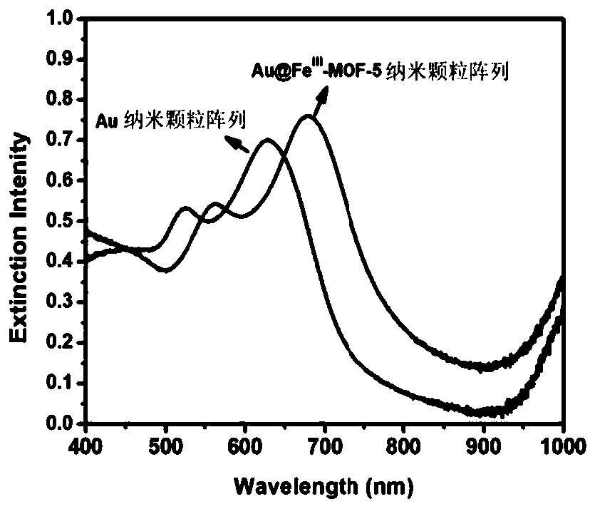
[0046] Such as Figure 6 As shown, a sensor for detecting the concentration of HCl gas is prepared by the following steps:
[0047] In step a, a single-layer polystyrene colloidal sphere crystal array is prepared on a quartz sheet through a gas-liquid interface self-assembly method.
[0048] Step b, using the quartz-based single-layer polystyrene colloidal sphere crystal array obtained in step a as a template, adopting the magnetron sputtering deposition method (the processing current of magnetron sputtering deposition is 20mA, the processing time of magnetron sputtering deposition The gold target material used in the 3min magnetron sputtering deposition meets the following conditions: a gold film with a thickness of 20-40 nm is deposited on the surface of the template.
[0049] Step c, put the above-mentioned template deposited with the gold film into a tube furnace, and heat and anneal at 900-1000° C. It will melt, fuse, and solidify in situ, thereby producing a periodic q...
PUM
| Property | Measurement | Unit |
|---|---|---|
| thickness | aaaaa | aaaaa |
Abstract
Description
Claims
Application Information


