Method for preparing flexible perovskite solar cell at low temperature,
A solar cell and perovskite technology, applied in the field of solar cells, can solve the problems of lower annealing temperature, high annealing temperature, and low cell efficiency, and achieve the effect of simple and controllable operation steps and simple process
- Summary
- Abstract
- Description
- Claims
- Application Information
AI Technical Summary
Problems solved by technology
Method used
Image
Examples
Embodiment 1
[0043] A method for preparing a light-absorbing layer of a perovskite solar cell, comprising the following steps:
[0044] Step 1. Select 1.5cm×1.5cm FTO conductive glass as the substrate, and use cleaning agent, acetone, ethanol and deionized water to clean it ultrasonically for 10 minutes. After cleaning, use nitrogen to dry the substrate, and then dry it. The FTO conductive glass is treated with oxygen plasma for 10 minutes to enhance the bonding force and adhesion on the surface of the substrate material;
[0045] Step 2. Dissolve 1.3mmol of lead iodide and 0.85mmol of formamidine iodide in a mixed solution of 1ml of dimethylsulfoxide (DMSO) and N,N-dimethylformamide (DMF), mix and stir After uniformity, place it on a heating platform to heat and dissolve at a temperature of 70° C., and then filter to prepare a solution A, wherein the volume percentage of DMF in the mixed solution is 80%, and the volume percentage of DMSO is 20%;
[0046] Step 3. Dissolve 0.15 mmol of met...
Embodiment 2
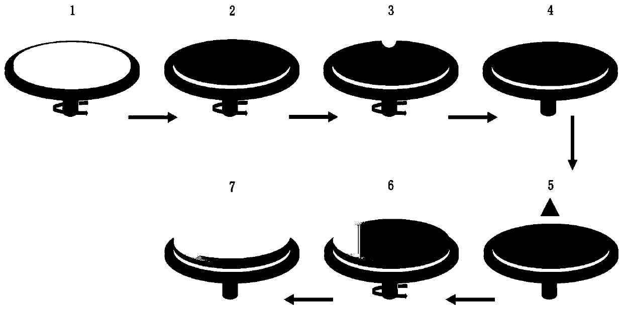
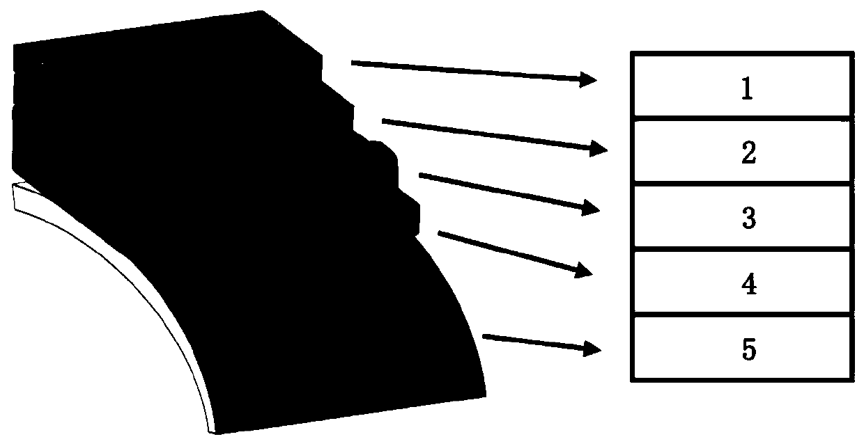
[0051] A method for preparing a flexible perovskite solar cell, comprising the following steps:
[0052] Step 1. Select 1.5cm×1.5cm PEN-ITO flexible conductive substrate (PEN is polyethylene naphthalate, ITO is tin-doped indium oxide), clean the surface with a small flow of nitrogen, and then Use oxygen plasma treatment for 2 minutes to enhance the bonding force and adhesion on the surface of the substrate material;
[0053] Step 2. Preparation of SnO 2 Electron transport layer: Dissolve nano-tin dioxide hydrosol with a volume ratio of 15% in distilled water and dilute to a solution with a volume percentage of 3.75%, and deposit it on the PEN-ITO flexible conductive layer obtained by step 1 by spin coating. On the material, sintering at a temperature of 90°C for 60 minutes, the dense SnO 2 Electron transport layer;
[0054] Step 3. Preparation of perovskite light absorbing layer:
[0055] 3.1. Dissolve 1.3mmol of lead iodide and 0.85mmol of formamidine iodide in 1ml of a m...
PUM
| Property | Measurement | Unit |
|---|---|---|
| Concentration | aaaaa | aaaaa |
| Thickness | aaaaa | aaaaa |
| Short circuit current density | aaaaa | aaaaa |
Abstract
Description
Claims
Application Information


