Optical sensing system and sensing testing method

A technology of optical sensing and optical sensor, which is applied in the field of optical sensing technology and sensors, can solve the problems of limited working wavelength range, photoelectric response band of silicon detectors, limited sensing performance of devices, limited sensing sensitivity, etc., and achieves increased The effect of large device operating wavelength range, enhanced detection responsivity, and wide operating wavelength range

Inactive Publication Date: 2019-09-20
JINAN UNIVERSITY
View PDF9 Cites 1 Cited by
  • Summary
  • Abstract
  • Description
  • Claims
  • Application Information

AI Technical Summary

Problems solved by technology

[0004] Although these works have achieved the functional integration of light sensing and light detection to a certain extent, they all require photodetector arrays, and they all use macroscopic assembling of light sensing chips and photodetectors. The cell pitch is large, and in sensing imaging applications, it will not work due to the crosstalk between adjacent pixels, which also limits the further miniaturization of the device volume
In addition, the resonant peaks of these sensor chips are very wide, the sensing sensitivity is limited, and their operating wavelength range is limited by the photoelectric response band of the silicon detector, which limits the applicable range of the device
[0005] In 2011, the journal OpticsExpress reported on page 9962, volume 19, an integrated optical sensor that prepared a metal nanopore structure on the surface of a silicon material pn junction photodetector covered with a silicon oxide layer. The measured object on the surface of the nanopore will change The characteristics of transmitted light, thus affecting the light absorption and photovoltage signal output of silicon materials
These have realized the monolithic integration of the sensing structure and the detection structure, and only a single detector is required. However, its working wavelength range is still limited by the transition mechanism between semiconductor bands, and the filtering performance of nanopores is limited by the large refractive index contrast. Severe interference at the bottom, resulting in indistinct resonance peaks, wide resonance peak linewidth, and low transmittance, resulting in small changes in the light absorption rate of the detector, which limits the sensing performance of the device, and the optical power and photocurrent of the voltage type device The linearity is poor, which is not conducive to sensing applications
[0006] It can be seen that although the existing technologies represented by the above examples have obtained optical sensing of electrical signal output, the test systems are relatively complex, and it is difficult to achieve high sensing sensitivity, narrow formant linewidth, and large operating wavelength range coexistence

Method used


Image

  • Optical sensing system and sensing testing method
  • Optical sensing system and sensing testing method
  • Optical sensing system and sensing testing method

Examples


Embodiment 1

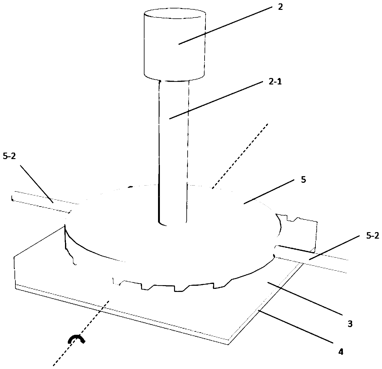
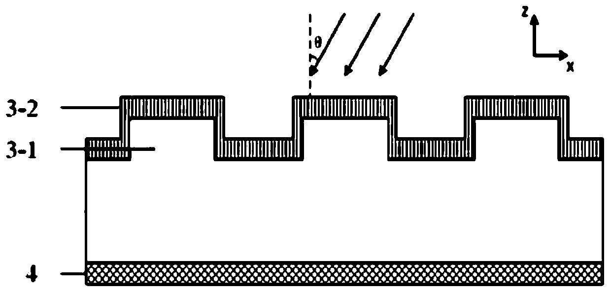
[0063] refer to figure 2 As shown, the first surface of the rotatable silicon wafer facing the monochromatic collimated light source forms a one-dimensional silicon material grating 3-1, wherein the period is 1 micron, the width of the silicon material grating 3-1 is 0.5 micron, and the depth of the silicon material grating is 35 nanometer; a gold film 3-2 is covered on the silicon material grating with a thickness of 50 nanometers. The silicon grating and the gold film together form the grating and form a Schottky junction, and the gold film serves as the first electrode of the photodetector. The second electrode 4 of the photodetector is formed on the second surface of the backlight of the silicon wafer, which is made of gold material and has a thickness of 200 nanometers.

[0064] The incident light of different wavelengths resonates with the surface plasmon wave of the grating 3 at a specific incident angle, and the resonance condition is determined by the following form...

Embodiment 2

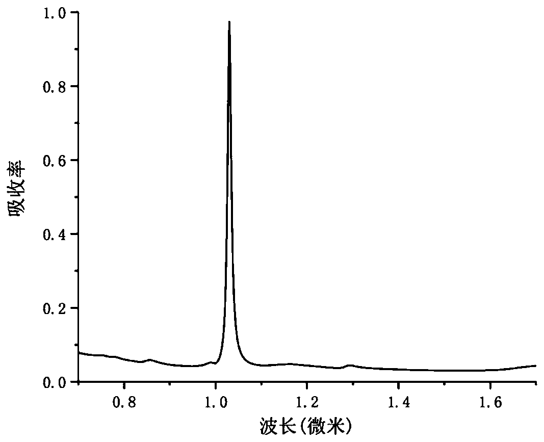
[0073] Figure 14 It is a schematic cross-sectional structure diagram of the photoelectric sensor in the angle-scanning electrical readout optical sensing system of this embodiment. Such as Figure 14 As shown, the preparation of the photodetector in the present embodiment is by covering the gold film on the surface of the rotating silicon wafer, and then forming a silicon dioxide grating 3-3 on the gold film, wherein the gold film thickness is 80 nanometers, and the silicon dioxide grating depth is 155 nm and the width is 360 nm. Figure 15 It is the calculation result of the absorption spectrum of the angle-scanning electrical readout optical sensing system of this embodiment under normal incident light irradiation. The resonance occurs at a wavelength of 1068 nm, the absorption at the peak is about 98%, the full width at half maximum is Figure 16 As shown, when the refractive index changes from 1 to 1.01, the resonance peak changes from 1068 nm to 1077 nm, and the sensit...

Embodiment 3

[0075] Figure 17 It is a schematic diagram of the photodetector in the electrical readout optical sensing system of the two-dimensional grating angular scanning of the present embodiment. In this embodiment, the photodetector is prepared by covering the surface of the rotating silicon wafer with a gold film, and then forming a gold two-dimensional disk array 3-4 on the gold film. The thickness of the gold film is 80 nanometers, the height of the two-dimensional gold disk array is 100 nanometers, the radius is 500 nanometers, and the disk period is 1400 nanometers. Figure 18 It is the calculation result of the absorption spectrum of the angle-scanning electrical readout optical sensing system of this embodiment under normal incident light irradiation. Resonance between incident light and surface plasmon waves occurs at 1412 nm at normal incidence. The absorption at the peak is greater than 98%, and the full width at half maximum is 4 nm. The quality factor Q is as high as ...


PUM

PropertyMeasurementUnit
Thicknessaaaaaaaaaa
Line widthaaaaaaaaaa
Divergence angleaaaaaaaaaa

Abstract

The invention discloses an optical sensing system. The optical sensing system comprises a monochromatic collimating light source, an optical sensor and a photoelectric detector; the photoelectric detector comprises a rotatable semiconductor substrate layer and a metal or metal-like material film covering the semiconductor substrate; the light facing surface of the photoelectric detector forms an optical grating; and the optical sensor and the photoelectric detector share the optical grating. The invention further discloses a sensing testing method using the optical sensing system. The sensing testing method comprises the following steps that: the monochromatic incident light source is started to irradiate; the semiconductor substrate layer is rotated, so that a resonance angle theta1 is obtained; an object to be detected is introduced, the semiconductor substrate layer is rotated, so that a resonance angle theta2 for irradiating the object to be tested is obtained; and the refractive index of the object to be tested can be obtained based on the change of the resonance angle theta2 relative to the resonance angle theta1. With the optical sensing system and sensing testing method of the invention adopted, high-sensing sensitivity, narrow-resonance peak line width and large-working wavelength range electric signal output can be realized, and the refractive index of gas or liquid can be measured with no extra spectrographs or photoelectric detectors required.

Description

technical field [0001] The invention relates to the field of optical sensing technology and sensors, in particular to an optical refraction index sensing system and a sensing test method that scans the angle of incident light and outputs it as a direct electrical signal. Background technique [0002] At present, there is an urgent demand for highly sensitive sensors in fields such as biomedicine, environmental monitoring, food safety and even national defense. Optical sensors have the characteristics of high sensitivity, anti-electromagnetic interference, and non-marking, so they have received extensive attention and vigorous development. Generally, optical sensors use optical resonance structures to enhance the sensing performance of the refractive index, and detect changes in the measured object by testing the wavelength shift of the resonance peak. The sensing sensitivity is defined as the wavelength shift of the resonant peak under the condition of the unit refractive i...

Claims


Application Information

Patent Timeline
IPC IPC(8): G01N21/41G01N21/552
CPCG01N21/41G01N21/554
Inventor 陈沁文龙
Owner JINAN UNIVERSITY
Why Eureka
Try Eureka