A method for preparing silicon epitaxial wafers for high-voltage power devices
A technology of high-voltage power devices and silicon epitaxial wafers, which is applied in the manufacture of semiconductor/solid-state devices, electrical components, coatings, etc., can solve the problems of out-of-control resistivity, discrete thickness distribution, and high defect density, and reduce the disturbance of resistivity , bright surface, the effect of increasing the reaction rate
- Summary
- Abstract
- Description
- Claims
- Application Information
AI Technical Summary
Problems solved by technology
Method used
Image
Examples
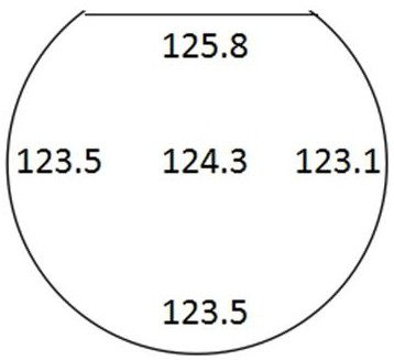
Embodiment 1
[0032] (1) Heat the base of the reaction chamber, set the temperature to 1180 °C, flow in hydrogen chloride gas for etching, set the flow rate to 18 L / min, and set the etching time to 240 sec. The residual substances deposited in the early stage of the base were removed by etching, and then the reaction chamber was purged with a large flow rate of 90 L / min hydrogen to remove the impurities etched from the base from the reaction chamber, and then the base was cleaned. Cool down to 60°C.
[0033] (2) Install the silicon substrate on the pedestal of the reaction chamber, heat the epitaxial pedestal, use a nonlinear gradient to raise the temperature of the silicon substrate to 1180°C, set the heating rate to 200°C / min, and heat up to The temperature was kept constant for 2 minutes at 800°C and 900°C, so that the thermal stress accumulated during the heating process could be released in time. A low flow rate of hydrogen chloride gas was introduced into the reaction chamber. The flo...
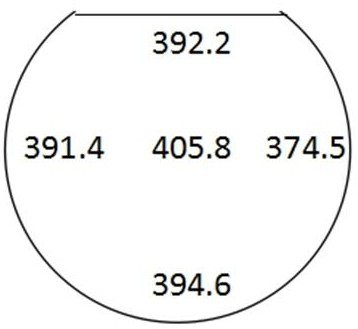
Embodiment 2
[0043] (1) Heat the base of the reaction chamber, set the temperature to 1180 °C, flow in hydrogen chloride gas for etching, set the flow rate to 18 L / min, and set the etching time to 240 sec. The residual substances deposited in the early stage of the base were removed by etching, and then the reaction chamber was purged with a large flow rate of 90 L / min hydrogen to remove the impurities etched from the base from the reaction chamber, and then the base was cleaned. Cool down to 60°C.
[0044] (2) Install the silicon substrate on the base of the reaction chamber, use a nonlinear gradient to raise the temperature of the silicon substrate to 1160°C, set the heating rate to 200°C / min, and when the temperature rises to 800°C and 900°C The average temperature was kept constant for 2 minutes, so that the thermal stress accumulated during the heating process could be released in time. A low flow rate of hydrogen chloride gas was introduced into the reaction chamber. The flow rate of...
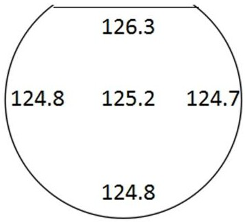
Embodiment 3
[0054] (1) Heat the base of the reaction chamber, set the temperature to 1180 °C, flow in hydrogen chloride gas for etching, set the flow rate to 18 L / min, and set the etching time to 240 sec. The residual substances deposited in the early stage of the base were removed by etching, and then the reaction chamber was purged with a large flow rate of 90 L / min hydrogen to remove the impurities etched from the base from the reaction chamber, and then the base was cleaned. Cool down to 60°C.
[0055] (2) Install the silicon substrate on the pedestal of the reaction chamber, heat the epitaxy pedestal, use a nonlinear gradient to raise the temperature of the silicon substrate to 1160°C, set the heating rate to 200°C / min, and heat up to The temperature was kept constant for 2 minutes at 800°C and 900°C, so that the thermal stress accumulated during the heating process could be released in time. A low flow rate of hydrogen chloride gas was introduced into the reaction chamber. The flow ...
PUM
| Property | Measurement | Unit |
|---|---|---|
| electrical resistivity | aaaaa | aaaaa |
| thickness | aaaaa | aaaaa |
| electrical resistivity | aaaaa | aaaaa |
Abstract
Description
Claims
Application Information
 - R&D
- Intellectual Property
- Life Sciences
- Materials
- Tech Scout
- Unparalleled Data Quality
- Higher Quality Content
- 60% Fewer Hallucinations
Browse by: Latest US Patents, China's latest patents, Technical Efficacy Thesaurus, Application Domain, Technology Topic, Popular Technical Reports.
© 2025 PatSnap. All rights reserved.Legal|Privacy policy|Modern Slavery Act Transparency Statement|Sitemap|About US| Contact US: help@patsnap.com


