Enhanced Ga2O3 metal oxide semiconductor field effect transistor and manufacturing method thereof

A technology of field-effect transistors and oxide semiconductors, which is applied in the field of microelectronics, can solve the problems of reducing the carrier concentration under the gate, etching damage on the surface of the concave gate, and affecting device performance, etc., so as to reduce the carrier concentration and reduce the Interface state density, the effect of improving device performance

Inactive Publication Date: 2020-01-14
XIDIAN UNIV
View PDF3 Cites 9 Cited by
  • Summary
  • Abstract
  • Description
  • Claims
  • Application Information

AI Technical Summary

Problems solved by technology

[0004] One is to adopt a fin-wound structure, that is, to form a parallel fin-shaped channel array by plasma etching, but the manufacturing process of this method is relatively complicated and the cost is high;
[0005] The second is to use inductively coupled plasma to etch the gate groove, that is, use BCl 3 Etching gas, by thinning the Ga in the gate region 2 o 3 The thickness of the channel layer reduces the carrier concentration under the gate, thereby realizing the enhanced Ga 2 o 3 For metal oxide semiconductor field effect transistors, etching by this method will cause etching damage on the surface of the concave gate and affect device performance

Method used


Image

  • Enhanced Ga2O3 metal oxide semiconductor field effect transistor and manufacturing method thereof
  • Enhanced Ga2O3 metal oxide semiconductor field effect transistor and manufacturing method thereof

Examples


Embodiment 1

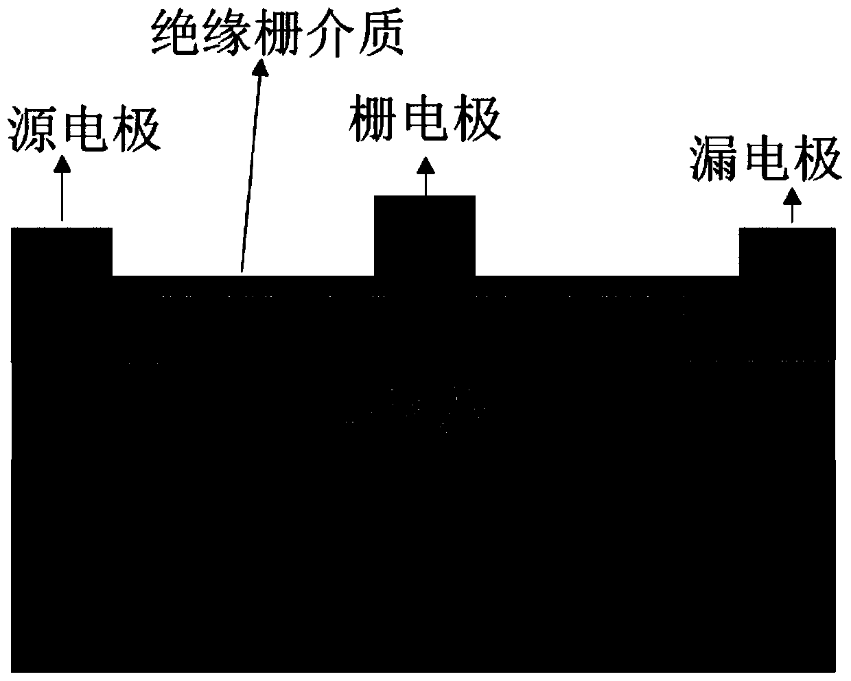
[0031] Embodiment 1, making n-type Ga 2 o 3 The thickness of the epitaxial layer is 150nm, and the electron concentration is 2.0×10 16 cm -3 , a field effect transistor with an insulating gate dielectric thickness of 10nm.

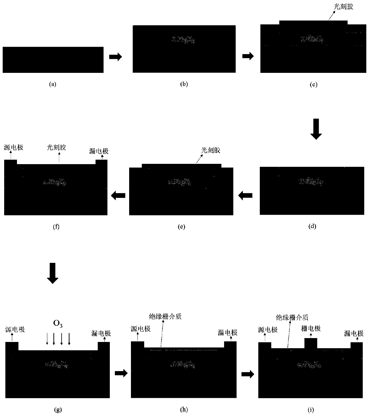
[0032] Step 1, cleaning the substrate, such as figure 2 (a).

[0033] The sapphire substrate is selected, cleaned with acetone solution first, then with ethanol solution, and finally with flowing deionized water and blown dry with high-purity nitrogen.

[0034] Step 2, grow n-type Ga on the substrate 2 o 3 epitaxial layer, such as figure 2 (b).

[0035] 2a) Put the cleaned sapphire substrate into the reaction chamber of the PLD equipment, set the partial pressure of oxygen in the reaction chamber to 0.01mbar, the temperature to 500°C, and the target material in the reaction chamber to be (AlGa) 2 o 3 , the distance between the sample to be grown and the target material is set to 4cm, and the energy density of the laser is set to 2J / cm 2 , the ...

Embodiment 2

[0055] Embodiment 2, making n-type Ga 2 o 3 The thickness of the epitaxial layer is 230nm, and the electron concentration is 2.0×10 17 cm -3 , a field effect transistor with an insulating gate dielectric thickness of 20nm.

[0056] Step 1, cleaning the substrate, such as figure 2 (a).

[0057] The specific implementation method of this step is the same as Step 1 in Example 1.

[0058] Step 2, growing n-type Ga on the substrate 2 o 3 epitaxial layer, such as figure 2 (b).

[0059] 2.1) Put the cleaned sapphire substrate into the reaction chamber of the PLD equipment, set the partial pressure of oxygen in the reaction chamber to 0.02mbar, the temperature to 600°C, and the target material in the reaction chamber to be (AlGa) 2 o 3 , the distance between the sample to be grown and the target material is set to 4cm, and the energy density of the laser is set to 3J / cm 2 , the pulse frequency is 4Hz, and the total number of pulses is 7000 times;

[0060] 2.2) The thickn...

Embodiment 3

[0078] Embodiment 3, making n-type Ga 2 o 3 The thickness of the epitaxial layer is 300nm, and the electron concentration is 1.0×10 18 cm -3 , a field effect transistor with an insulating gate dielectric thickness of 30nm.

[0079] Step A, the substrate is cleaned, such as figure 2 (a).

[0080] Mg-doped Ga 2 o 3 The substrate was first cleaned with acetone solution, then with ethanol solution, and finally with flowing deionized water and dried with high-purity nitrogen.

[0081] Step B, growing n-type Ga on the substrate 2 o 3 epitaxial layer, such as figure 2 (b).

[0082] Put the cleaned sapphire substrate into the reaction chamber of the PLD equipment first, and use the method of laser deposition to grow on the substrate with a thickness of 300nm and an electron concentration of 1.0×10 18 cm -3 n-type Ga 2 o 3 film, to obtain n-type Ga 2 o 3 epitaxial layer.

[0083] The growth process conditions are: the oxygen partial pressure in the reaction chamber i...


PUM

PropertyMeasurementUnit
thicknessaaaaaaaaaa
thicknessaaaaaaaaaa
thicknessaaaaaaaaaa

Abstract

The invention discloses an enhanced Ga2O3 metal oxide semiconductor field effect transistor and a manufacturing method thereof, which mainly solve the problem of complex manufacturing of similar devices in the prior art. The enhanced Ga2O3 metal oxide semiconductor field effect transistor comprises a substrate, an epitaxial layer and an insulated gate dielectric layer from bottom to top; a sourceelectrode and a drain electrode are arranged on the epitaxial layer, and a gate electrode is arranged on the insulated gate dielectric layer. The thickness of the insulated gate dielectric layer is 10-30 nm; the epitaxial layer is an n-type Ga2O3 epitaxial layer, the thickness being 150-300 nm, and the electron concentration being 2.0 * 10 < 16 >-1.0 * 10 < 18 > cm <-3 >. The manufacturing key ofthe device is that before an insulated gate dielectric layer is deposited, the temperature of a cavity is set to be 200-500 DEG C, and O3 is introduced into an ALD reaction cavity to treat the surfaceof an n-type Ga2O3 channel layer for 5-15 min. The interface state density and static power consumption of the device are reduced, the threshold voltage is increased, the manufacturing cost and difficulty are reduced, and the method can be used for power devices and high-voltage switching devices.

Description

technical field [0001] The invention belongs to the technical field of microelectronics, in particular to a Ga 2 o 3 Metal-oxide-semiconductor transistors that can be used in power devices and high-voltage switching devices. Background technique [0002] Ga 2 o 3 As a wide bandgap semiconductor material, it has five isomers, of which monoclinic β-type Ga 2 o 3 The stability is the best, the bandgap width is about 4.8eV-4.9eV, and the theoretical breakdown electric field can reach 8MV / cm, which is twice more than the other two excellent wide bandgap semiconductor materials, silicon carbide and gallium nitride. The Liga excellent value is 3444, which is eight times that of silicon carbide and four times that of gallium nitride. Therefore Ga 2 o 3 It is a wide bandgap semiconductor material with excellent performance suitable for the preparation of power devices and high-voltage switching devices. [0003] The enhanced type is a necessary condition to ensure the stable...

Claims


Application Information

Patent Timeline
Patent Type & Authority Applications(China)
IPC IPC(8): H01L29/78H01L21/425H01L21/34C23C16/455C23C16/40C23C14/30C23C14/18C23C14/16
CPCC23C14/16C23C14/18C23C14/30C23C16/40C23C16/45525H01L21/425H01L29/66969H01L29/78
Inventor 冯倩崔晨霞蔡云匆封兆青胡壮壮田旭升张进成郝跃
Owner XIDIAN UNIV
Why Eureka
Try Eureka