A composite material negative electrode, battery and preparation method thereof
A composite material and negative electrode technology, which is applied in the field of batteries, can solve the problems of unfavorable electrode rate performance, promotion, and limited electrochemical active sites, so as to improve space utilization, suppress dendrite self-amplification parasitic growth, and promote tendencies The effect of leveling
- Summary
- Abstract
- Description
- Claims
- Application Information
AI Technical Summary
Problems solved by technology
Method used
Image
Examples
preparation example Construction
[0033] According to another embodiment of the present invention, a method for preparing a composite negative electrode includes the following steps:
[0034] S1. Using polymer materials or inorganic oxides as raw materials to prepare non-conductive porous dielectric layers;
[0035] S2. Using carbon materials or metal materials as raw materials to prepare a porous conductive layer;
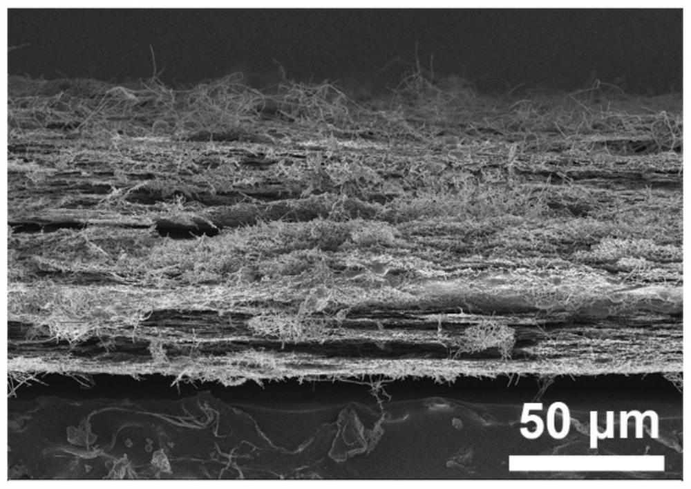
[0036] S3. Assembling the porous dielectric layer and the porous conductive layer periodically to prepare a three-dimensional framework with alternating conductive / dielectric cycles, preferably by layer-by-layer stacking or layer-by-layer suction filtration or magnetron sputtering performing said cycle assembly;
[0037] S4. Composite the active metal with the three-dimensional framework, and embed the active metal inside the three-dimensional framework to obtain the negative electrode of the composite material.
[0038] The sequence of steps S1 and S2 in the above preparation method is not limite...
Embodiment 1
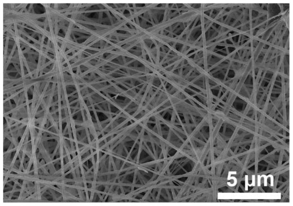
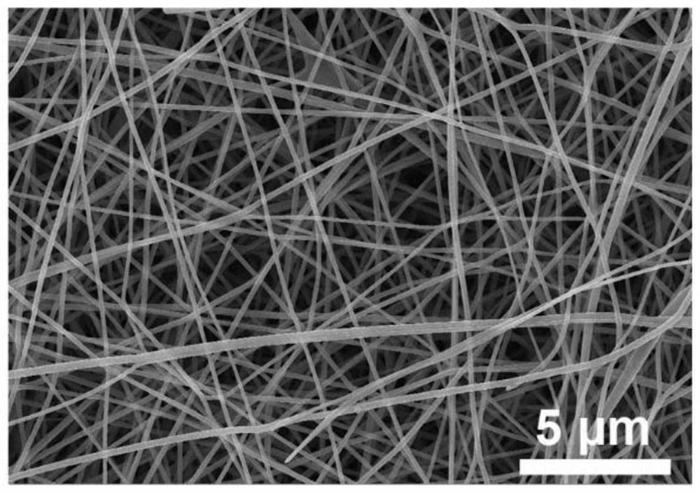
[0066] Dissolving the PAN powder in the DMF solvent, stirring for 0.5-72 hours, and preparing a polymer liquid with a solid content of 2%-50%. Subsequently, the configured precursor solution was electrospun on the aluminum foil by injection through a syringe; the electrospun PAN was peeled off from the surface of the aluminum foil to obtain the skeleton of the dielectric fiber membrane. By controlling the electrospinning time, a PAN film with a thickness of 2-50 microns is obtained for the dielectric skeleton.
[0067]The PAN obtained by electrospinning was carbonized to obtain the conductive CNF framework material. The carbonization process is as follows: the first step, in the air atmosphere, place the PAN film in a furnace at 100-500 °C for 0.5-5 hours for pre-oxidation, and then cool it to room temperature with the furnace; the second step, in the argon atmosphere The pre-oxidized PAN film is kept at 800-1500° C. for 0.5-5 hours, then cooled to room temperature, and the h...
Embodiment 2
[0079] SiO with a diameter of 1-20 microns 2 The small ball particles are dispersed in the N,N-dimethylformamide (DMF) solution of polyamic acid (PAA), and the solid content of the solution is kept within the range of 2% to 50%; height to prepare PAA films of different thicknesses. Silica spheres are uniformly dispersed in the PAA film. Then, at a heating rate of 1-10°C / min, heat at 60-500°C for 0.5-720 minutes to pretreat and remove the solution, and hold at 60-500°C for 0.5-720 minutes to thermally imidize PAA to obtain a polyimide (PI) film , the thickness of the dielectric PI film is controlled within the range of 2-50 microns.
[0080] The PI film prepared above was soaked in hydrofluoric acid for 12 hours, the hydrofluoric acid reacted with the silica pellets, and etched to obtain a dielectric PI film with internal pores. The thickness of the porous PI film after etching is maintained within the range of 2-50 microns; the pore size and porosity inside the porous PI fi...
PUM
| Property | Measurement | Unit |
|---|---|---|
| diameter | aaaaa | aaaaa |
| diameter | aaaaa | aaaaa |
| thickness | aaaaa | aaaaa |
Abstract
Description
Claims
Application Information


