Novel GaN junction barrier Schottky diode and preparation method thereof

A junction barrier Schottky and diode technology, which is applied in semiconductor/solid-state device manufacturing, electrical components, circuits, etc., can solve the problems of increasing the difficulty and complexity of the device process, limiting the development of JBS structure devices, and high electric field strength at the edge of the positive electrode. , to achieve the effect of reducing the difficulty and complexity of the process, the effect is remarkable, and the breakdown performance is enhanced

Inactive Publication Date: 2020-02-04
CHANGCHUN INST OF OPTICS FINE MECHANICS & PHYSICS CHINESE ACAD OF SCI
View PDF8 Cites 2 Cited by
  • Summary
  • Abstract
  • Description
  • Claims
  • Application Information

AI Technical Summary

Problems solved by technology

The traditional Schottky diode has the following defects: (1) When the reverse blocking capability is close to 200V, the forward voltage drop V of the Schottky rectifier F will be close to the forward voltage drop of the PIN rectifier, so the reverse blocking voltage of the traditional Schottky barrier diode is generally lower than 200V, making it less efficient in the application
(2) The traditional Schottky diode has a large reverse leakage current and is sensitive to temperature. The junction temperature of the traditional Schottky diode is between 125°C and 175°C
[0004] Existing JBS devices need to etch the n-type epitaxial layer to re-grow the p-type epitaxial layer in the n-type epitaxial layer, and require multiple annealing at a temperature of up to 1100°C to complete the activation of the p-type epitaxial layer, which greatly increases The process difficulty and complexity of the device limit the development of gallium nitride-based JBS structure devices
In addition, similar to Schottky barrier diodes (SBDs), the electric field strength at the positive edge of JBS is high, which can easily cause reverse breakdown of the device

Method used


Image

  • Novel GaN junction barrier Schottky diode and preparation method thereof
  • Novel GaN junction barrier Schottky diode and preparation method thereof
  • Novel GaN junction barrier Schottky diode and preparation method thereof

Examples


Embodiment Construction

[0029] The present invention will be described in further detail below in conjunction with the accompanying drawings and embodiments.

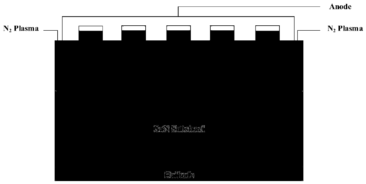
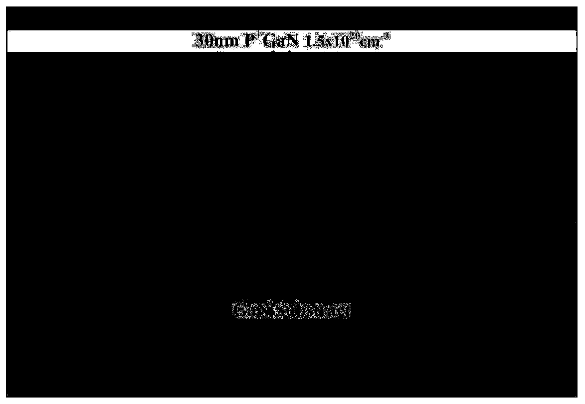
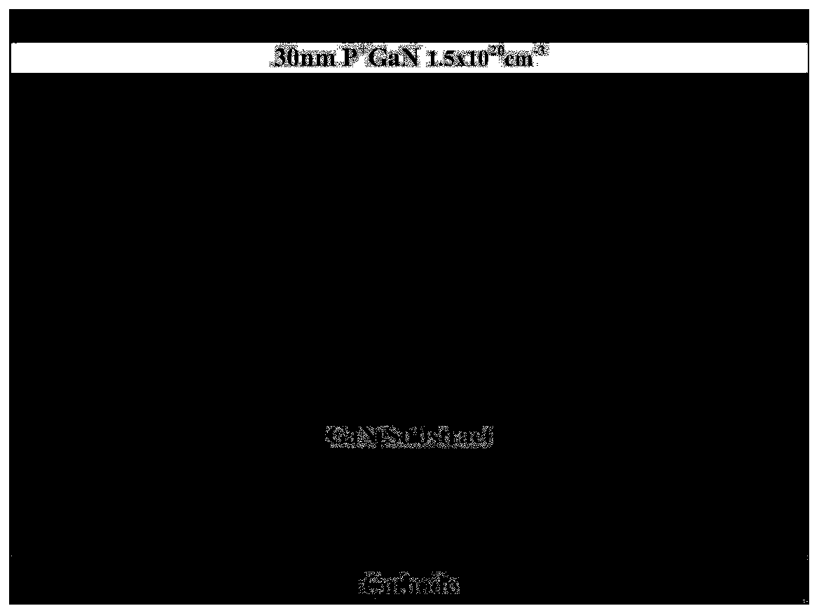
[0030] Such as figure 1 As shown, the new GaN junction barrier Schottky diode, the diode from bottom to top includes: cathode, substrate, n + type GaN epitaxial layer, n-type GaN epitaxial layer, a high resistance region formed by annular injection of plasma on the outer edge of the n-type GaN epitaxial layer, comb-shaped p-type GaN epitaxial layer, comb-shaped p + type GaN epitaxial layer and anode. The material of the substrate may be: gallium nitride, silicon and silicon carbide substrates. the n + type GaN epitaxial layer, n-type GaN epitaxial layer, comb-shaped p-type GaN epitaxial layer and comb-shaped p + The growth method of the type GaN epitaxial layer is organic chemical vapor deposition or hydride vapor phase epitaxy. In this example, the n + Type GaN epitaxial layer thickness is 2μm, carrier concentration is about 1.5x10 18 ...


PUM

PropertyMeasurementUnit
thicknessaaaaaaaaaa
thicknessaaaaaaaaaa
thicknessaaaaaaaaaa

Abstract

The invention discloses a novel GaN junction barrier Schottky diode and a preparation method thereof, which provides a new way for improving the performance of the Schottky diode by utilizing a noveldesign and a relatively simple and easily-achieved process. The novel GaN junction barrier Schottky diode sequentially comprises a cathode, a substrate, an n+ type GaN epitaxial layer, an n type GaN epitaxial layer, a high-resistance region, a comb-shaped p type GaN epitaxial layer, a comb-shaped p+ type GaN epitaxial layer and an anode from bottom to top, wherein plasmas are annularly injected into the outer edge of the n type GaN epitaxial layer to form the high-resistance region. According to the invention, p-type GaN does not need to be grown in the n-type GaN layer and a subsequent activation process is not needed, so that the process difficulty and the complexity are greatly reduced. Through the four layers of epitaxial GaN structures, good ohmic contact and better PN junctions can be formed, the forward on resistance is reduced, the reverse breakdown voltage is increased, and the performance of the device is effectively improved. In addition, the high-resistance region formed byN2 Plasma can effectively inhibit breakdown of the device at the edge of an electrode under high voltage, and the breakdown performance is enhanced.

Description

technical field [0001] The invention belongs to the technical field of semiconductors, in particular to a novel GaN junction barrier Schottky diode and a preparation method thereof. Background technique [0002] In recent years, due to the low turn-on voltage drop and extremely short reverse recovery time of Schottky Barrier Diodes (SBDs), the improvement of circuit system efficiency has attracted great attention and has been widely used. The traditional Schottky diode has the following defects: (1) When the reverse blocking capability is close to 200V, the forward voltage drop V of the Schottky rectifier F will be close to the forward voltage drop of the PIN rectifier, so the reverse blocking voltage of the traditional Schottky barrier diode is generally lower than 200V, making it less efficient in the application. (2) The traditional Schottky diode has a large reverse leakage current and is sensitive to temperature. The junction temperature of the traditional Schottky dio...

Claims


Application Information

Patent Timeline
Patent Type & Authority Applications(China)
IPC IPC(8): H01L29/872H01L29/06H01L21/329
CPCH01L29/0611H01L29/0615H01L29/0657H01L29/66143H01L29/872
Inventor 黎大兵刘新科孙晓娟贾玉萍石芝铭
Owner CHANGCHUN INST OF OPTICS FINE MECHANICS & PHYSICS CHINESE ACAD OF SCI
Why Eureka
Try Eureka