Erbium silicate waveguide amplifier based on on-chip pumping and preparation method thereof

A technology of waveguide amplifier and erbium silicate, which is applied in the field of optoelectronics, can solve the problems of difficulty in growing indium phosphide, poor performance and reliability of optoelectronic devices, thermal mismatch of semiconductors, etc., so as to avoid basic difficulties and meet high-density integration , The effect of reducing the size of the device

Active Publication Date: 2020-02-11
PEKING UNIV
View PDF8 Cites 8 Cited by
  • Summary
  • Abstract
  • Description
  • Claims
  • Application Information

AI Technical Summary

Problems solved by technology

However, scaling these devices down and integrating them with silicon photonics poses significant challenges
For erbium-doped optical fiber amplification materials and devices, due to the small optical cross-section of erbium ions themselves (~10 -21 cm 2 ) and low solid solubility (20 cm -3 ), causing the optical gain per unit distance it can provide is very small, so that the erbium-doped fiber usually needs a distance of several meters or even longer to provide sufficient gain for the optical signal
When the erbium-doped optical gain material is made into an optical waveguide and integrated on a silicon substrate, although the optical gain per unit distance (~dB / cm) can be improved, it is still necessary to make the optical waveguide into a spiral shape to have a long enough operating distance while occupying as small an area as possible, which is contrary to the requirements of high-density integration
On the other hand, since most erbium-doped optical gain materials are insulating media (doping erbium into silicon and other semiconductors has been studied for many years but has never achieved real optical gain), the conductivity is poor, and it is difficult to perform direct electrical injection excitation, so the integrated erbium-doped optical waveguide amplifier device still needs an external pump light source, which makes the optoelectronic integration scheme very complicated
[0004] If the semiconductor optical amplifier in the 1.55 μm band uses InGaAsP material that matches the indium phosphide (InP) lattice, its integration with silicon optical chips will face two major difficulties: first, in terms of materials, The lattice mismatch between indium phosphide and silicon reaches about 8%, and the polarity is different. It is very difficult to directly epitaxially grow indium phosphide and indium gallium arsenic phosphide on a silicon substrate, and the grown material has a high defect density. Produced optoelectronic devices with poor performance and reliability
However, using hybrid integration methods such as bonding and film transfer, although higher-quality III-V devices can be obtained, due to the difference between the indium phosphide substrate (up to 3 inches) and the silicon substrate (12 inches is the mainstream in the industry) There is a large difference in size, and there are problems in wafer-level integration and processing
Moreover, hybrid integration also faces the problem of thermal mismatch between III-V semiconductors and silicon
Second, in terms of performance, semiconductor optical amplifiers also have inherent problems. Because the lifetime of the upper energy level carriers is too short, it will cause a large gain compression and recovery effect with the pulse density distribution of the data stream. The amplifier is used to amplify the modulated optical signal itself has a large defect

Method used


Image

  • Erbium silicate waveguide amplifier based on on-chip pumping and preparation method thereof
  • Erbium silicate waveguide amplifier based on on-chip pumping and preparation method thereof
  • Erbium silicate waveguide amplifier based on on-chip pumping and preparation method thereof

Examples


Embodiment Construction

[0041] In order to make the purpose, technical solutions and advantages of the embodiments of the present invention clearer, the technical solutions in the embodiments of the present invention will be clearly and completely described below in conjunction with the drawings in the embodiments of the present invention. Obviously, the described embodiments It is a part of embodiments of the present invention, but not all embodiments. Based on the embodiments of the present invention, all other embodiments obtained by persons of ordinary skill in the art without creative efforts fall within the protection scope of the present invention.

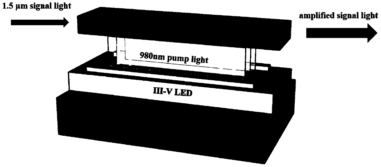
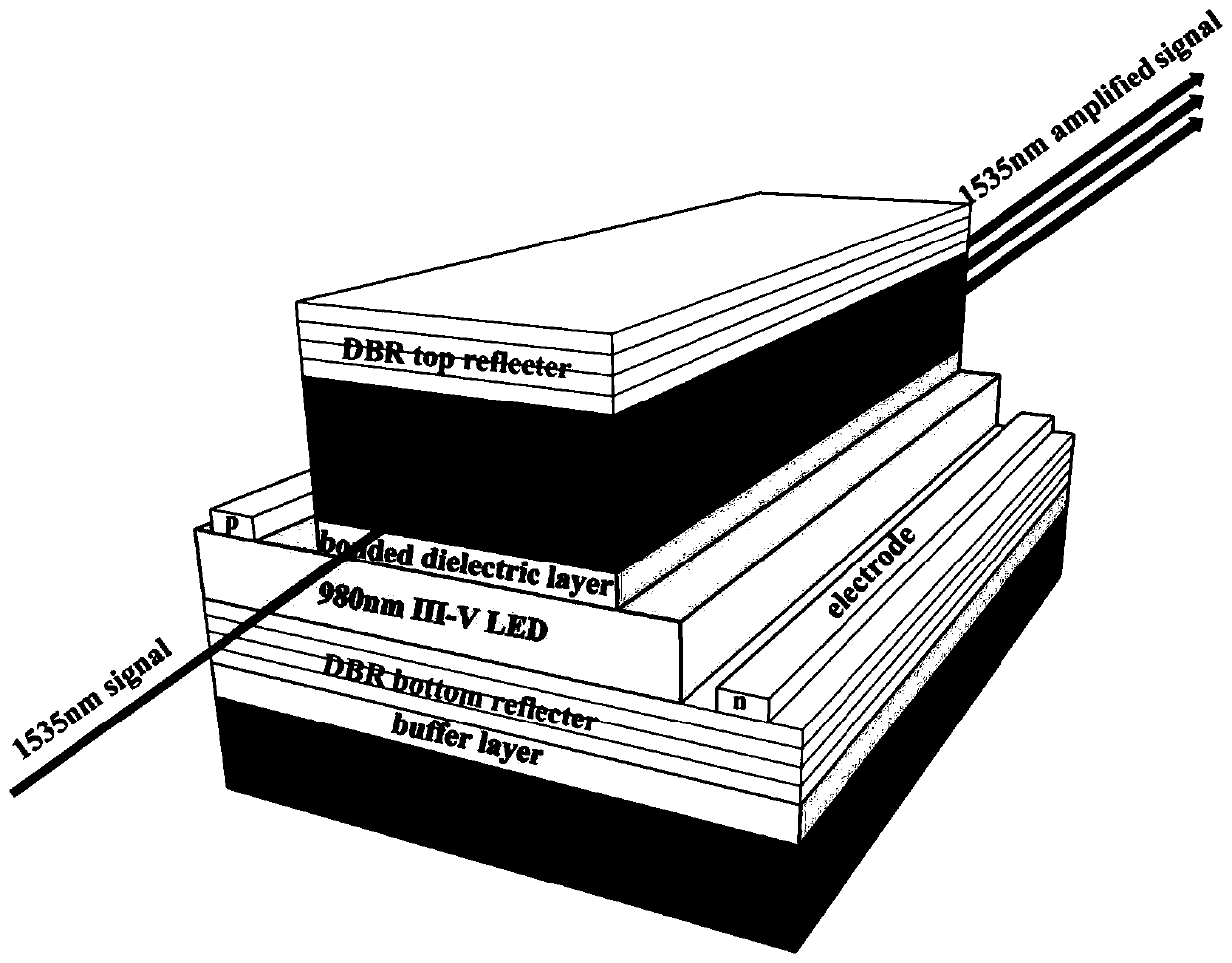
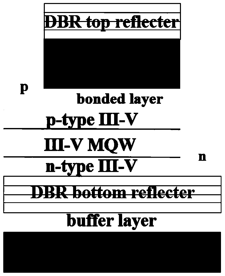
[0042] At present, silicon photonics technology has entered a mature stage, but reliable silicon-based light sources such as lasers and optical amplifiers are still short boards; in addition, erbium-doped materials are recognized as suitable materials for optical amplifiers, but erbium-doped optical amplifiers cannot be directly pumped Pu.

[004...


PUM

PropertyMeasurementUnit
reflectanceaaaaaaaaaa

Abstract

The embodiment of the invention provides an erbium silicate waveguide amplifier based on on-chip pumping and a preparation method of the erbium silicate waveguide amplifier. The amplifier comprises asilicon substrate, a DBR bottom reflector, a pump light source, a gain medium layer and a DBR top reflector which are sequentially arranged on a light path, wherein the DBR bottom reflector and the DBR top reflector form a DBR resonant cavity, the pump light source is used for generating pump light through electroluminescence, the transmission direction of the pump light intersects with the transmission direction of the signal light passing through the gain medium layer, and the DBR resonant cavity is used for performing resonance enhancement of the pump light. The erbium silicate waveguide amplifier is advantaged in that by integrating an erbium silicate gain dielectric layer and a III-V group LED active layer, an III-V group semiconductor light source improves electro-optical conversionefficiency, improves light absorption and pumping efficiency of a gain material, introduces a reliable light source device for a silicon photonic system, and provides the high-speed and large-capacityoptical signal amplification basis for an optical amplifier.

Description

technical field [0001] The invention relates to the field of optoelectronic technology, in particular to an erbium silicate waveguide amplifier based on on-chip pumping and a preparation method thereof. Background technique [0002] In the past ten years, silicon photonics has made great progress. Low-loss optical waveguides, high-speed optical modulators, and high-speed transceiver modules based on silicon photonics technology have gradually become practical, making silicon photonics technology widely used in optical communications and data centers. The application in fields such as the industry is gradually becoming clear, and the commercialization has entered the implementation stage. It has become a consensus in academia and industry that silicon photonics technology will play an important role in the current and future fields of high-speed and large-capacity information transmission and processing. Among the many functional devices that make up the silicon photonics sy...

Claims


Application Information

Patent Timeline
Patent Type & Authority Applications(China)
IPC IPC(8): H01S3/0933H01S3/16
CPCH01S3/0933H01S3/1608H01S3/1655
Inventor 王兴军周佩奇王冰何燕冬
Owner PEKING UNIV
Why Eureka
Try Eureka