

Method of preparing silicon carbide MOSFET gate dielectric layer
A gate dielectric layer, silicon carbide technology, applied in electrical components, circuits, semiconductor devices, etc., can solve the problems of C cluster aggregation, high thermal budget of SiO2 gate dielectric layer, low dielectric constant, etc., to reduce the electric field strength, simplify the Device fabrication process, effect of high dielectric constant
- Summary
- Abstract
- Description
- Claims
- Application Information
AI Technical Summary
Problems solved by technology
Method used
Image

Examples
Embodiment 1
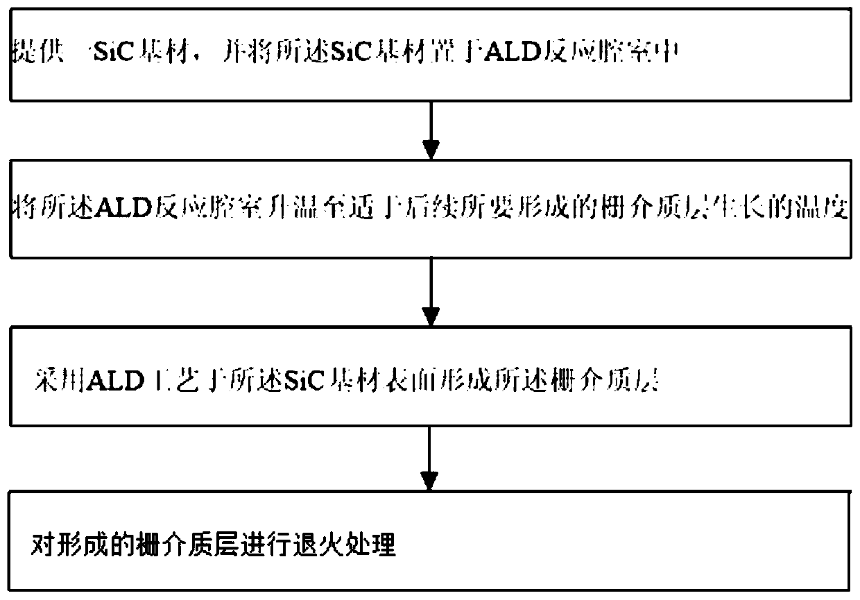
[0052] Such as figure 1 As shown, the present invention provides a method for preparing a silicon carbide MOSFET gate dielectric layer, comprising the following steps:
[0053] S1: Provide the SiC substrate and place the SiC substrate in the ALD reaction chamber;
[0054] S2: heating the ALD reaction chamber;
[0055] S3: Using the ALD process to sequentially grow SiO on the surface of the SiC substrate 2 thin film and Al 2 o 3 thin film to form a gate dielectric layer.
[0056] S4: performing annealing treatment on the formed gate dielectric layer in an oxygen atmosphere.
[0057] A method for preparing a silicon carbide MOSFET gate dielectric layer according to the present invention will be described in detail below with reference to the accompanying drawings.
[0058] Such as figure 1 As shown in S1, perform step S1, provide a SiC substrate, and place the SiC substrate in the ALD reaction chamber;
[0059] Specifically, the SiC substrate includes but is not limited ...
Embodiment 2
[0107] Such as figure 1 As shown, the present invention provides a method for preparing a silicon carbide MOSFET gate dielectric layer, comprising the following steps:
[0108] S1: Provide the SiC substrate and place the SiC substrate in the ALD reaction chamber;
[0109] S2: heating the ALD reaction chamber;
[0110] S3: Using the ALD process to sequentially grow SiO on the surface of the SiC substrate 2 thin film and Al 2 o 3 thin film to form a gate dielectric layer.
[0111] S4: performing annealing treatment on the formed gate dielectric layer in an oxygen atmosphere.
[0112] A method for preparing a silicon carbide MOSFET gate dielectric layer according to the present invention will be described in detail below with reference to the accompanying drawings.
[0113] Such as figure 1 As shown in S1, perform step S1, provide a SiC substrate, and place the SiC substrate in the ALD reaction chamber;
[0114] Specifically, the SiC substrate includes but is not limited ...
Embodiment 3
[0162] Such as figure 1 As shown, the present invention provides a method for preparing a silicon carbide MOSFET gate dielectric layer, comprising the following steps:
[0163] S1: Provide the SiC substrate and place the SiC substrate in the ALD reaction chamber;
[0164] S2: heating the ALD reaction chamber;
[0165]S3: Using the ALD process to sequentially grow SiO on the surface of the SiC substrate 2 thin film and Al 2 o 3 thin film to form a gate dielectric layer.
[0166] S4: performing annealing treatment on the formed gate dielectric layer in an oxygen atmosphere.
[0167] A method for preparing a silicon carbide MOSFET gate dielectric layer according to the present invention will be described in detail below with reference to the accompanying drawings.
[0168] Such as figure 1 As shown in S1, perform step S1, provide a SiC substrate, and place the SiC substrate in the ALD reaction chamber;
[0169] Specifically, the SiC substrate includes but is not limited t...
PUM
| Property | Measurement | Unit |
|---|---|---|
| strength | aaaaa | aaaaa |
| thickness | aaaaa | aaaaa |
| strength | aaaaa | aaaaa |
Abstract
Description
Claims
Application Information