A method for making optical micro-nano pattern on the surface of lithium niobate thin film

A technology for surface fabrication and lithium niobate, which is applied in the photo-engraving process of optics and pattern surface, and the exposure device of photo-engraving process, etc., can solve the problems of affecting electron beam deflection, increasing device size, and large optical mode field size, etc. Accurate and controllable pattern size, reduced optical device size, and large refractive index contrast

Active Publication Date: 2021-02-26
TSINGHUA UNIV +1
View PDF6 Cites 0 Cited by
  • Summary
  • Abstract
  • Description
  • Claims
  • Application Information

AI Technical Summary

Problems solved by technology

[0004] (1) Titanium diffusion and proton exchange methods can only produce optical waveguides with small refractive index difference (<0.02), resulting in weak confinement of optical signals, large optical mode field size, reduced optical device performance, and increased device size
[0005] (2) In the titanium diffusion process, Li is easy to diffuse outward from the substrate surface, and the Li-deficient surface will produce a z-polarized planar waveguide, which seriously affects the performance of optical devices.
The proton exchange process can only be applied to x-cut and z-cut lithium niobate wafers, because the acid solution will cause chemical corrosion to y-cut wafers
In addition, proton exchange can only increase the refractive index of abnormal light, and high-temperature annealing treatment is required to solve the problems of unstable refractive index and attenuation of electro-optic effect
[0006] (3) The size of the graphics produced by lithography can only be made to more than 1 μm, and fine graphics cannot be processed
[0008] PMMA electron beam glue has the characteristics of high resolution, high contrast and low sensitivity, but its etching resistance is poor. When making nanostructures, due to the fine pattern, it is necessary to evenly coat thinner PMMA glue, which is even weaker. The anti-etching performance of PMMA cannot be achieved in dry etching
HSQ (hydrogen silsesquioxane) electron beam glue is a kind of negative glue with extremely high resolution. It is widely used in electron beam exposure, but its sensitivity to electrons is very low, so it needs electron beam in electron beam exposure. Increased dose and time limit its larger application
[0009] In addition, most light-transmitting materials used in the optical field have low electrical conductivity, which leads to charge accumulation during electron beam exposure, which affects the deflection of the electron beam, resulting in pattern defects and drift
Therefore, this problem is usually solved by making a thin (10-15nm) metal conductive layer on the upper surface of the substrate with low conductivity, but this will make electrons more likely to drift laterally and affect the steepness of the side wall of the pattern. Spend

Method used


Image

  • A method for making optical micro-nano pattern on the surface of lithium niobate thin film
  • A method for making optical micro-nano pattern on the surface of lithium niobate thin film

Examples


Embodiment Construction

[0045] In order to make the object, technical solution and advantages of the present invention clearer, the present invention will be further described in detail below in conjunction with the accompanying drawings and embodiments. It should be understood that the specific embodiments described here are only used to explain the present invention, not to limit the present invention.

[0046] The electron beam exposure machine used in this embodiment is produced by UK Nanobeam Co., Ltd., and the model is NB5.

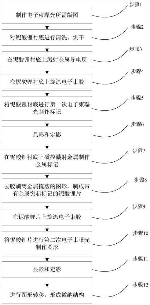
[0047] A method for making optical micro-nano patterns on the surface of a lithium niobate thin film, such as figure 1 shown, including the following steps:

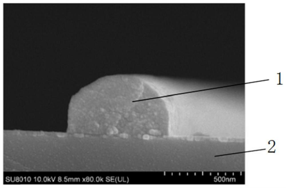
[0048]Step 1, making a layout required for electron beam exposure in drawing software (such as AutoCAD or Ledit, etc.), and the layout includes first-layer marks and second-layer graphics. The first layer is marked as a square with a side length greater than 4 μm, or a cross with a width greater than 4 μm, wherein ...


PUM

PropertyMeasurementUnit
thicknessaaaaaaaaaa
thicknessaaaaaaaaaa
thicknessaaaaaaaaaa

Abstract

The invention relates to a method for manufacturing an optical micro-nano pattern on the surface of a lithium niobate film, which belongs to the technical field of micro-nano processing. The method comprises the following steps: manufacturing a layout required by electron beam exposure; cleaning and drying a lithium niobate substrate; sputtering a metal conductive layer on the lithium niobate substrate; spin-coating the lithium niobate substrate with electron beam glue; carrying out first electron beam exposure on the lithium niobate substrate to manufacture a mark; carrying out developing andfixing; carrying out magnetron sputtering of metal on the lithium niobate substrate to manufacture a metal mark; removing the photoresist and stripping a metal-masked pattern to prepare a lithium niobate sheet with a metal bulge mark; spin-coating the lithium niobate sheet with electron beam glue; carrying out second electron beam exposure on the lithium niobate sheet to manufacture a pattern; carrying out developing and fixing; and carrying out pattern transfer to form a micro-nano structure. By means of the method, a pattern with a steep side wall can be manufactured on a non-conductive lithium niobate material, a micro-nano pattern with the size smaller than 900nm can be manufactured, the manufactured optical waveguide is large in refractive index contrast ratio, the size of an opticaldevice can be reduced, and the performance of the optical device can be improved.

Description

technical field [0001] The invention relates to a method for making optical micro-nano patterns on the surface of a lithium niobate thin film, belonging to the technical field of micro-nano processing. Background technique [0002] Lithium niobate material (LiNbO 3 ) is a non-conductive uniaxial crystal. Due to its wide light transmission window (340-4600nm) and excellent electro-optic, acousto-optic, nonlinear optics, and piezoelectric properties, it is widely used in the fields of optical signal processing, quantum electrodynamics, and optomechanics. with broadly application foreground. Single crystal lithium niobate thin films can be prepared by ion implantation and bonding technology. Due to the emergence of lithium niobate thin films, lithium niobate materials have received more attention in the field of integrated optics. [0003] At present, the fabrication methods of lithium niobate optical waveguide mainly include titanium diffusion and proton exchange after photo...

Claims


Application Information

Patent Timeline
Patent Type & Authority Patents(China)
IPC IPC(8): G03F7/20
CPCG03F7/2022G03F7/2059
Inventor 曾嵘庄池杰马昕雨沈瞿欢王华磊吴长春
Owner TSINGHUA UNIV
Why Eureka
Try Eureka