
Double-layer metal waveguide coupling surface plasma resonance chip and preparation method thereof

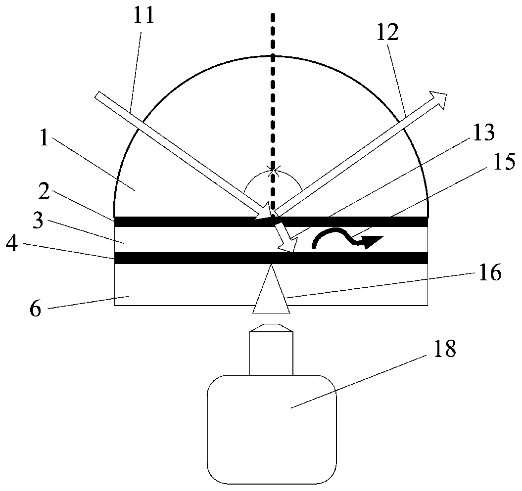
A surface plasmon, double-layer metal technology, applied in the field of spectral analysis and detection, can solve the problems of limited analysis and detection sensitivity, low spectral quality, etc., and achieve the effects of improving detection sensitivity, enhancing SERS signal, and good protection.

Inactive Publication Date: 2020-03-13
CHANGCHUN INST OF OPTICS FINE MECHANICS & PHYSICS CHINESE ACAD OF SCI
View PDF1 Cites 4 Cited by
  • Summary
  • Abstract
  • Description
  • Claims
  • Application Information

AI Technical Summary

Problems solved by technology

[0004] Based on this, it is necessary to provide a double-layer metal waveguide coupled surface plasmon resonance chip and its preparation method to improve Spectral quality of surface-enhanced Raman scattering signals, improving analytical detection sensitivity

Method used


Image

  • Double-layer metal waveguide coupling surface plasma resonance chip and preparation method thereof
  • Double-layer metal waveguide coupling surface plasma resonance chip and preparation method thereof
  • Double-layer metal waveguide coupling surface plasma resonance chip and preparation method thereof

Examples


preparation example Construction

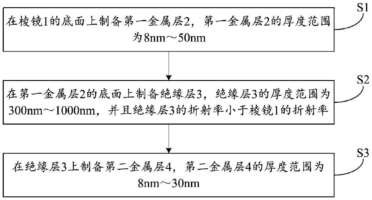
[0026] In one example, see figure 1 , the invention discloses a method for preparing a double-layer metal waveguide coupling surface plasmon resonance chip, which includes the following steps:

[0027] Step S1: preparing a first metal layer 2 on the bottom surface of the prism 1, the thickness of the first metal layer 2 is in the range of 8nm-50nm. Preferably, the material of the first metal layer 2 is various metals such as gold, silver, copper, aluminum, platinum, and palladium. The prism 1 can be a triangular prism with different sizes and different refractive indices, a semi-cylindrical cylindrical mirror or a hemispherical prism, and the material of the prism 1 is optical glass.

[0028] Step S2 : preparing an insulating layer 3 on the bottom surface of the first metal layer 2 , the thickness of the insulating layer 3 ranges from 300 nm to 1000 nm, and the refractive index of the insulating layer 3 is smaller than that of the prism 1 . Preferably, the material of the in...

Embodiment 1

[0043] According to the Fresnel equation and multilayer film theory, the electric field distribution and reflectivity formula on the surface of the metal film under the multilayer film SPR structure can be simulated. The basic principle is described as follows:

[0044] For a multilayer film system composed of prisms and multilayer dielectric substances, the medium between the high refractive index cylindrical mirror and the semi-infinite dielectric substrate can be treated as a multilayer medium. The dielectric constants of the cylindrical mirror and the semi-infinite dielectric substrate are respectively ε p and ε s to represent that the dielectric constant of the jth layer medium is ε j , with thickness d j . When a beam of plane light waves is incident on the interface between the cylindrical mirror and the multilayer medium through the cylindrical prism at an incident angle θ, the incident beam 19 is decomposed into a reflected beam 21 and a transmitted beam at the int...

Embodiment 2

[0048] Using the relevant formula of electromagnetic field propagation in the medium, the electric field under the traditional SPR structure constructed by the three layers of semi-cylindrical mirror / silver film / water (here water is used as the sample layer and silver is used as the material of the metal layer) in each layer The distribution of the semi-cylindrical mirror is simulated, and the material of the semi-cylindrical mirror is K9 glass, the refractive index is 1.52, and the thickness of the silver film is 45nm. The simulation results are as follows Figure 7 As shown, the abscissa in the figure is the distance in the Z direction (unit is nm), and the ordinate is the electric field intensity. Depend on Figure 7 It can be seen that the penetration depth of the electric field of the traditional SPR structure is 510 nm.

[0049] Next, this embodiment simulates a double-layer metal waveguide coupled surface plasmon resonance chip. Magnesium layer / silver film, using wate...


PUM

PropertyMeasurementUnit
Thicknessaaaaaaaaaa
Thicknessaaaaaaaaaa
Thicknessaaaaaaaaaa

Abstract

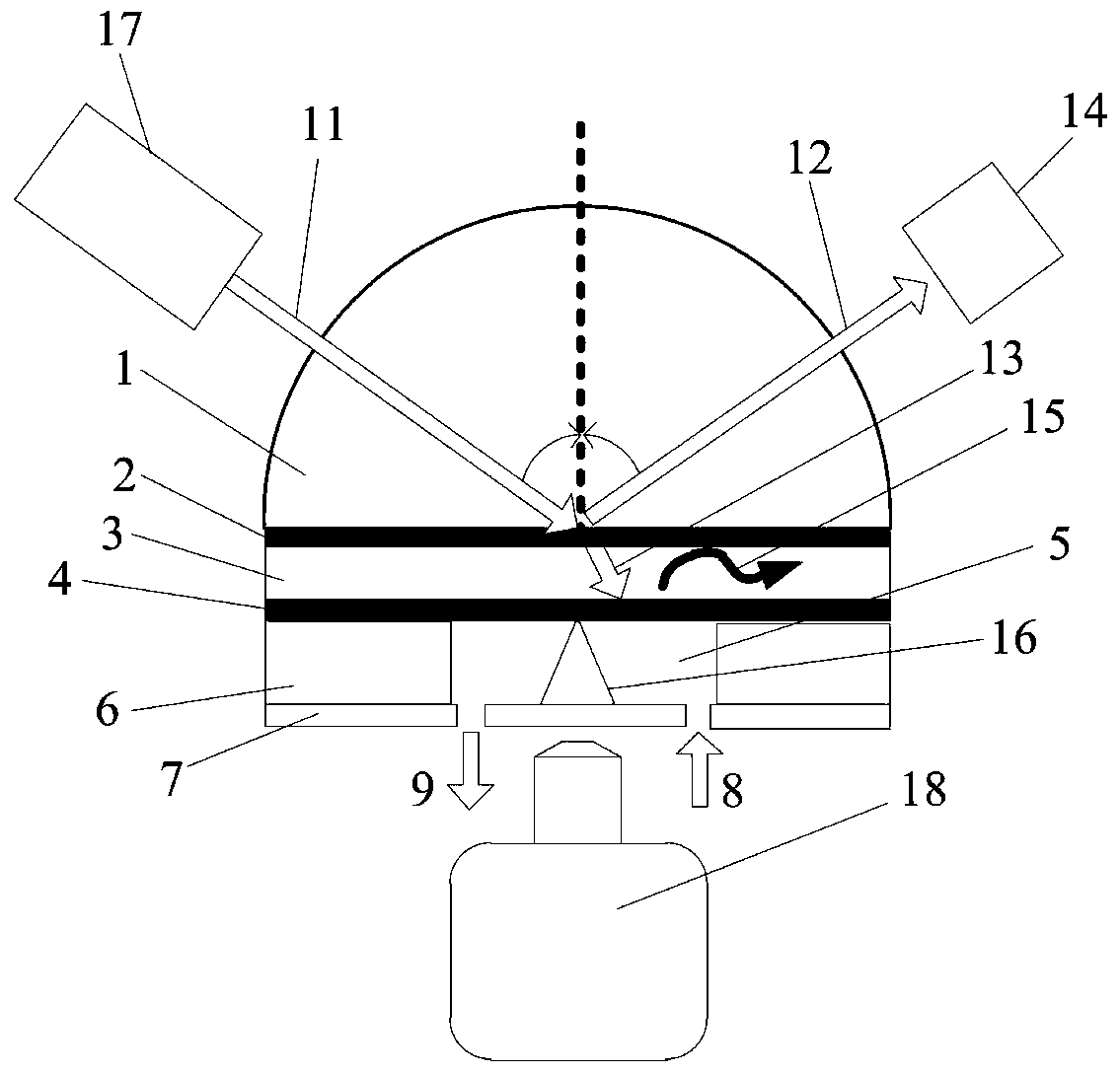
The invention relates to a double-layer metal waveguide coupling surface plasma resonance chip and a preparation method thereof. The preparation method comprises the steps that a first metal layer isprepared on the bottom surface of a prism, and the thickness of the first metal layer ranges from 8 nm to 50 nm; an insulating layer is prepared on the bottom surface of the first metal layer, the thickness of the insulating layer ranges from 300 nm to 1000 nm, and the refractive index of the insulating layer is smaller than that of the prism; and a second metal layer is prepared on the insulatinglayer, and the thickness of the second metal layer ranges from 8 nm to 30 nm. According to the invention, the SERS signal is greatly enhanced; SERS detection sensitivity is further improved; waveguide coupling SPR is used for exciting SERS, so the SPR resonance angle is small, and the requirement for an excitation device is low; and meanwhile, the penetration depth of an electric field in a detected object is large, a protective layer can be constructed on the surface of a metal layer, and therefore an SPR metal sensing film is better protected.

Description

technical field [0001] The invention belongs to the technical field of spectral analysis and detection, and in particular relates to a double-layer metal waveguide coupled surface plasmon resonance chip and a preparation method thereof. Background technique [0002] Surface-enhanced Raman spectroscopy (SERS) refers to the enhancement of metal nanomaterials and structures up to 10 4 -10 10 Raman signal. At present, it is generally believed that the physical enhancement of SERS is mainly due to surface plasmon resonance (Surface-plasmon Resonance, SPR). Surface plasmons (SurfacePlasmon, SP) are essentially light waves that interact with free electrons on the surface of a conductor and are trapped on the surface. The incident light forces the free electrons on the surface of the conductor to form a collective vibration, and when the collective vibration frequency is consistent with the frequency of the incident light, a resonance is formed, which is called surface plasmon re...

Claims


Application Information

Patent Timeline
IPC IPC(8): G01N21/65
CPCG01N21/658
Inventor 刘钰张海涛王丽萍
Owner CHANGCHUN INST OF OPTICS FINE MECHANICS & PHYSICS CHINESE ACAD OF SCI
Learn More