

Damage-free high-planarity monocrystalline silicon carbide planar optical element and preparation method thereof
A technology of single crystal silicon carbide and optical components, which is applied in the direction of optical surface grinders, grinding/polishing equipment, manufacturing tools, etc., can solve problems such as difficult processing, and achieve small density, high elastic modulus, and excellent thermal conductivity. Effect
- Summary
- Abstract
- Description
- Claims
- Application Information
AI Technical Summary
Problems solved by technology
Method used
Image


Examples
preparation example Construction
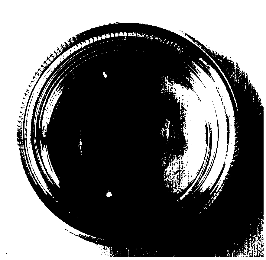
[0047] The preparation method of the present invention is aimed at the single crystal optical element required by the application in the optical field. The shape is generally a relatively thick block. In addition to the high flatness and low damage index, the surface processing also needs to meet the application index in the optical field at the same time. Such as ultra-low optical flatness. Therefore, the crystal plane and optical processing technology are strictly limited in terms of processing methods, especially the introduction of small grinding head chemical mechanical polishing optical plane modification technology, and the non-damaging high optical precision modification of the local protruding parts of the surface is carried out in a targeted manner, so as to obtain both Mirror surface with damage-free and high optical flatness.
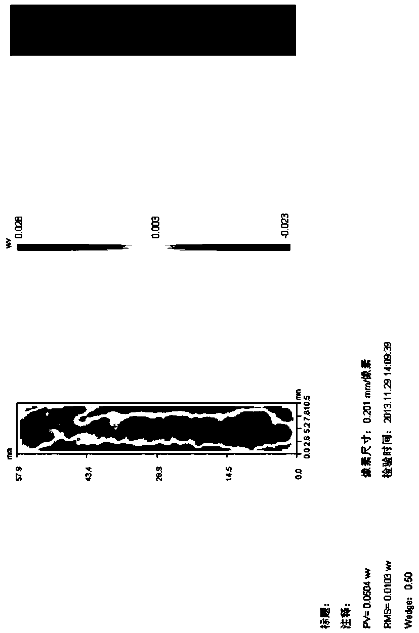
[0048] Flatness parameters are generally used in semiconductor single wafers, usually in microns (μm), and the flatness of a general wafer ...
Embodiment 1
[0055] The preparation of a non-damaging, high-flatness single-crystal silicon carbide planar optical element based on single-crystal silicon carbide materials is achieved by the following steps:
[0056] (1) Select a 4-inch 4H crystal form high-purity single-crystal silicon carbide ingot grown by the physical vapor transport (PVT) method. The main impurity components are nitrogen (N) and boron (B), and the concentrations are N=6E16 atoms / cm 3 , B=2E15 atoms / cm 3 ;
[0057] (2) Use a surface grinder to carry out surface grinding on the two large growth surfaces with large areas of the crystal ingot (here, the surface with an off-angle with the (001) surface within 10 degrees), and use a double-sided polishing machine to perform rough polishing to obtain Bright two end faces;
[0058] (3) Use a polarizer to carry out optical inspection on the end face, and select silicon carbide crystal ingots without micropipes;
[0059] (4) Orienting the selected silicon carbide crystal ...
Embodiment 2-5
[0072] It is basically the same as in Example 1, except that the doping content of the doping chemical elements B and V is adjusted to prepare a planar optical element from the single crystal silicon carbide. Wherein the silicon carbide single crystal doping component in embodiment 2 is N, B, and concentration is N=6E16atoms / cm 3 ,B=4E15 atoms / cm 3 , the corresponding curve (b) of its optical transmittance; the silicon carbide single crystal doping component in embodiment 3 is N, B, V, and concentration is N=6E16 atoms / cm 3 ,B=4E15 atoms / cm 3 , V=5E16 atoms / cm 3, its optical transmittance corresponding curve (c); SiC single crystal doping components are N, B, V in embodiment 4, concentration is N=6E16atoms / cm 3 ,B=4E15 atoms / cm 3 , V=1E17 atoms / cm 3 , the corresponding curve (d) of its optical transmittance; the silicon carbide single crystal doping component is N, B, V in the embodiment 5, and the concentration is N=6E16 atoms / cm 3 ,B=4E15 atoms / cm 3 , V=2E17atoms / cm ...
PUM
| Property | Measurement | Unit |
|---|---|---|
| Surface roughness | aaaaa | aaaaa |
| Surface roughness | aaaaa | aaaaa |
| Surface roughness | aaaaa | aaaaa |
Abstract
Description
Claims
Application Information