Manufacturing method of printed circuit conductive circuit

A conductive circuit and printed circuit technology, which is applied in the field of printed circuit board manufacturing, can solve the problems of inability to meet the requirements of high-frequency and high-speed signal transmission, uneven and rough erosion of circuit graphics, and inability to realize mass production, etc., to avoid The production cost is too high, avoid rough and uneven, and avoid the effect of poor thermal stability

A conductive circuit and printed circuit technology, which is applied in the field of printed circuit board manufacturing, can solve the problems of inability to meet the requirements of high-frequency and high-speed signal transmission, uneven and rough erosion of circuit graphics, and inability to realize mass production, etc., to avoid The production cost is too high, avoid rough and uneven, and avoid the effect of poor thermal stability

CN111405771APending Publication Date: 2020-07-10UNIV OF ELECTRONIC SCI & TECH OF CHINA

Image

  • Manufacturing method of printed circuit conductive circuit
  • Manufacturing method of printed circuit conductive circuit
  • Manufacturing method of printed circuit conductive circuit

Examples


Embodiment 1

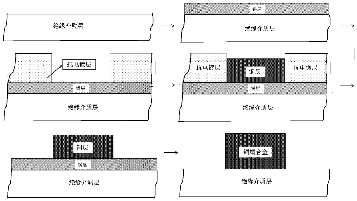
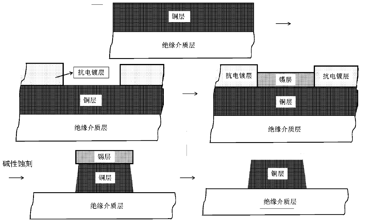
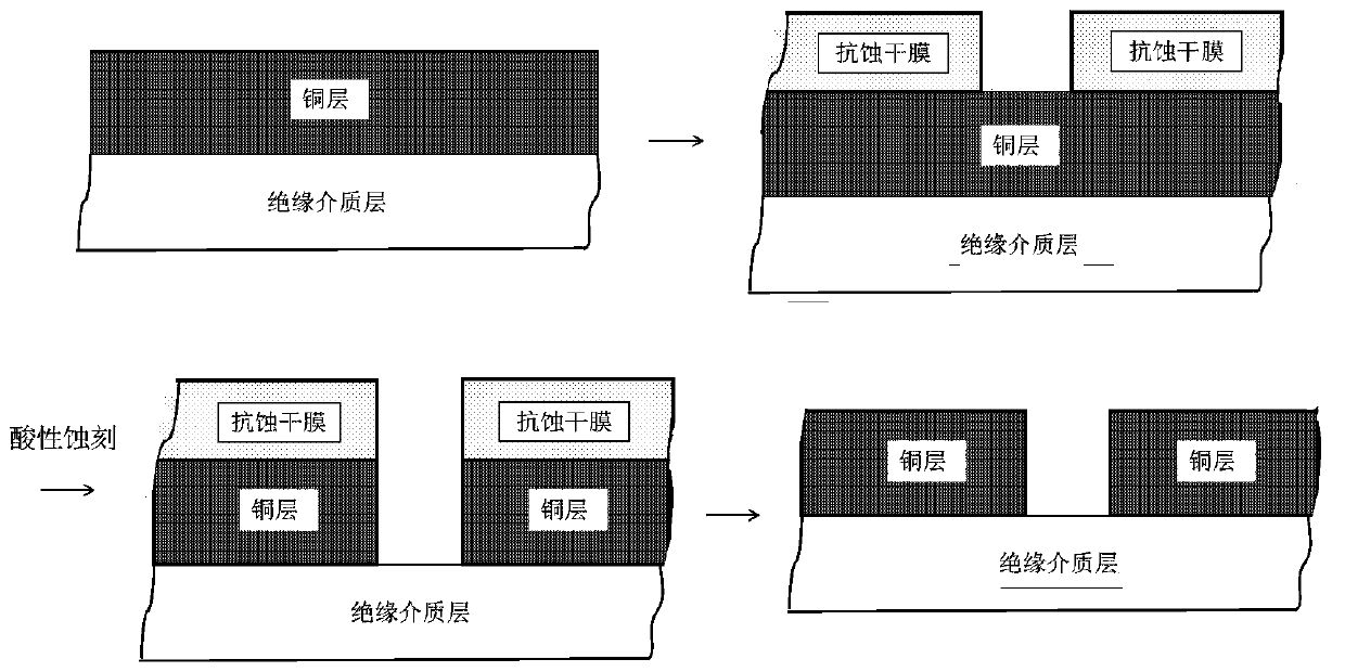
[0039] Cut the epoxy resin substrate of 20mm*100mm, after the plasma surface treatment, according to the plating solution formula shown in Table 1, the tin seed layer with a thickness of 2 μm is grown on the surface of the substrate by electroless tin plating by immersion plating; after the growth is completed, Cover the patterned dry film; then carry out electroplating copper according to the plating solution formula shown in Table 2, form copper conductive lines on the tin seed layer area not covered by the dry film on the substrate surface, and 5wt% hydrogen at 60 ° C Remove the dry film in the sodium oxide solution; then heat-treat at 180°C for 30s, take it out and cool it to room temperature naturally after heat treatment; finally, etch the tin seed layer area not covered by the electroplated copper layer to obtain the printed circuit conductive circuit.

[0040] The plating bath formula of table 1 growth tin seed layer

[0041] Bath composition concentration ...

Embodiment 2

[0047] Compared with Example 1, the present embodiment differs in that: the PI (Polyimide, polyimide) of 15mm*100mm is used as the substrate, and the surface treatment method is soaked in the KOH solution of 1mol / L for 10 minutes, and the remaining steps are the same as Example 1 is the same.

Embodiment 3

[0049] Compared with Example 1, this embodiment differs in that: use 15mm*100mm PET (PolyethyleneTerephthalate, polyethylene terephthalate) as the substrate, and soak in 1mol / L KOH solution for 10 minutes as surface treatment mode, and the rest of the steps are the same as in Example 1.


PUM

PropertyMeasurementUnit
Thicknessaaaaaaaaaa
Thicknessaaaaaaaaaa
Thicknessaaaaaaaaaa

Abstract

The invention discloses a manufacturing method of a printed circuit conductive circuit, and relates to the technical field of printed circuit board manufacturing. The method comprises the following steps: (1) growing a tin seed layer on the surface of a printed circuit insulating substrate; (2) covering the tin seed layer with a patterned dry film; (3) electroplating copper to form a copper conductive circuit; (4) removing the dry film; (5) carrying out heat treatment on the substrate obtained after the treatment in the previous step, so that the copper conductive circuit and the tin seed layer are co-melted into a whole; and 6) etching the tin seed layer to obtain a printed circuit conductive circuit. According to the method, the tin layer etching speed is high, the precision is high, thecircuit is complete and free of side etching, and manufacturing of a high-precision circuit board is facilitated; meanwhile, the copper and the tin are eutectic to form a uniform alloy layer, so thatthe stress between the metals is released, the local defect caused by inconsistent etching speeds of the tin seed layer and the copper conductive wire is prevented, the binding force of the conductive circuit and a bottom layer insulating medium is ensured, and the circuit pattern is good in heat resistance, high in stability and high in reliability.

Description

technical field [0001] The invention relates to the technical field of printed circuit board manufacturing, in particular to a method for manufacturing a conductive circuit of a printed circuit. Background technique [0002] As a "bridge" for carrying electronic components and connecting circuits, printed circuit boards are widely used in communication electronics, consumer electronics, computers, automotive electronics, industrial control, medical equipment, national defense and aerospace and other fields. indispensable existence. In recent years, under the accelerated evolution of cloud technology, 5G network construction, big data, artificial intelligence, sharing economy, industry 4.0, Internet of Things, etc., the market has put forward higher requirements for PCB manufacturing technology. Density, high precision, and miniaturization require that its manufacturing technology and process urgently need reform and innovation, and the first thing to bear the brunt is the p...

Claims


Application Information

Patent Timeline
10 Jul 2020
Publication
CN111405771A
IPC
H05K3/06
CPC
H05K3/06
Inventors
王守绪; 胡甲聪