Electronic component package and method for producing same

一种电子部件、制造方法的技术,应用在半导体/固态器件制造、电气元件、电固体器件等方向,能够解决镀敷层剥落、未涉及系统级封装等问题

Pending Publication Date: 2020-08-04
DIC CORP
View PDF1 Cites 19 Cited by
  • Summary
  • Abstract
  • Description
  • Claims
  • Application Information

AI Technical Summary

Problems solved by technology

For example, Patent Document 1 discloses an electronic component package equipped with a plurality of plating layers as layers for shielding electromagnetic wave noise, but does not refer to system-in-package
[0003] However, although the above-mentioned electronic component package is provided with a plating layer as a shielding layer directly on the sealing body that seals the electronic components, there is a disadvantage that the plating layer is easily peeled off from the sealing body.

Method used


Image

  • Electronic component package and method for producing same
  • Electronic component package and method for producing same
  • Electronic component package and method for producing same

Examples


Embodiment

[0095] Hereinafter, the present invention will be described in detail through examples.

[0096] (Preparation example 1: Preparation of metal particle dispersion liquid)

[0097] In a mixed solvent of 30 parts by mass of ethylene glycol and 70 parts by mass of ion-exchanged water, a compound obtained by adding polyethylene oxide to polyethyleneimine was used as a dispersant to disperse silver particles with an average particle diameter of 30 nm, and then add Water, ethanol, and surfactant were ion-exchanged, and the viscosity was adjusted to 10 mPa·s to prepare a metal particle dispersion. It should be noted that the metal particle dispersion liquid contains metal particles and a polymer dispersant having a nitrogen atom-containing basic group as a reactive functional group.

manufacture example 1

[0098] (Manufacturing example 1: Manufacture of polymer layer resin)

[0099] In a reaction vessel equipped with a stirrer, a reflux cooling pipe, a nitrogen gas introduction pipe, and a thermometer, in a mixed solvent of 111 parts by mass of methyl ethyl ketone, polycarbonate polyol (1,4-cyclohexanedimethanol and 100 parts by mass of polycarbonate diol having an acid group equivalent of 1,000 g / equivalent), 9.7 parts by mass of 2,2-dimethylolpropionic acid, and 5.5 parts by mass of 1,4-cyclohexanedimethanol obtained by the carbonate reaction 51.4 parts by mass of dicyclohexylmethane diisocyanate were reacted to obtain an organic solvent solution of a urethane prepolymer having an isocyanate group at a molecular terminal.

[0100]Next, by adding 7.3 parts by mass of triethylamine to the organic solvent solution of the above-mentioned polyurethane resin to neutralize part or all of the carboxyl groups contained in the above-mentioned polyurethane resin, and further adding 355 p...

Embodiment 1

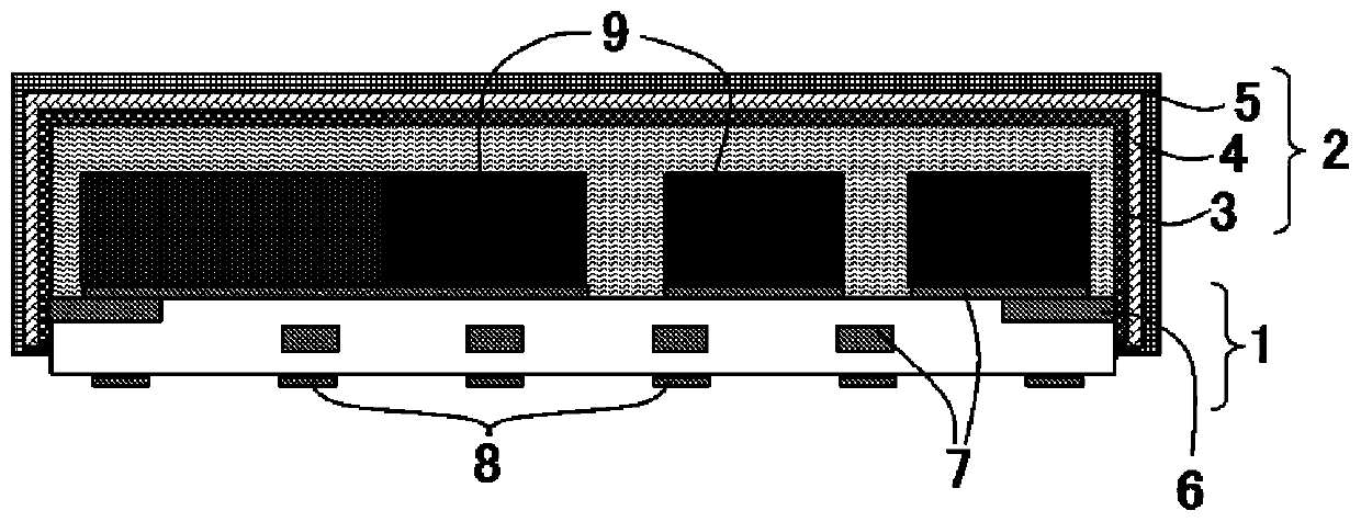
[0107] An electronic component mounted on a circuit board having a ground pattern is sealed with a resin composition for encapsulating a semiconductor containing an epoxy resin, a phenolic resin curing agent, and a filler. On the surface of the sealing body, the metal particle dispersion liquid prepared in Preparation Example 1 was coated with a spray device (a spray device equipped with a spray tip QTKA (flow size: 0.1 L / min) of a nozzle manufactured by Spraying Systems Japan Co., Ltd.). The film thickness after drying as the metal particle layer was 150 nm. Then, it was dried at 180° C. for 10 minutes to form a metal particle layer. The surface resistance value of this metal particle layer was 4Ω / □.

[0108] Next, on the metal particle layer formed by the above method, phosphorus-containing copper is set as an anode, and an electroplating solution containing copper sulfate is used at a current density of 2.5A / dm 2 Copper electroplating was performed for 10 minutes to lamin...


PUM

PropertyMeasurementUnit
particle diameteraaaaaaaaaa
viscosity indexaaaaaaaaaa

Abstract

The present invention provides an electronic component package and a method for producing the same. The electronic component package comprises: an electronic component that is mounted on a circuit substrate having a ground pattern; a sealing body that contains an epoxy resin and seals the electronic component; and a shield layer that is formed on the sealing body. This electronic component packageis characterized in that: the shield layer is obtained by sequentially stacking, from the sealing body side, a metal particle layer, a copper plating layer and a nickel plating layer; and the shieldlayer is grounded to the ground pattern. This electronic component package is excellent in terms of adhesion of the shield layer.

Description

technical field [0001] The present invention relates to an electronic component package and a method of manufacturing the same. Background technique [0002] In recent years, so-called system-in-package (SiP) semiconductors that operate as one functional block by mounting an IC and multiple electronic components in a single semiconductor package have been widely used in portable information terminals such as smartphones. encapsulation. Such a semiconductor package prevents malfunctions due to external noise and also takes measures against electromagnetic wave noise so that it does not itself become a noise source. For example, Patent Document 1 discloses an electronic component package including a plurality of plating layers as a layer for shielding electromagnetic wave noise, but does not relate to a system-in-package. [0003] However, the above-mentioned electronic component package has a disadvantage that the plating layer is easily peeled off from the sealing body, al...

Claims


Application Information

Patent Timeline
Patent Type & Authority Applications(China)
IPC IPC(8): H01L23/28H01L21/56H01L23/00
CPCH01L23/3142H01L23/3121H01L21/561H01L2924/15313H01L2924/3025H01L2924/15311H01L2224/97H01L2224/32225H01L23/552H01L24/32H01L24/97H01L2224/83H01L23/60H01L23/31H01L23/293H01L23/06H01L23/5286H01L23/50
Inventor 白发润深泽宪正
Owner DIC CORP
Why Eureka
Try Eureka