A boron-doped diamond electrode with high conductivity, long life and high specific surface area, its preparation method and application

A high specific surface area, diamond electrode technology, applied in the direction of electrodes, chemical instruments and methods, electrolytic components, etc., can solve the problems of unfavorable solution mass transfer, strong oxidizing active groups, small specific surface area, low electrode efficiency, etc., to achieve low Effects of residual stress, increase in specific surface area, and increase in adhesion

Active Publication Date: 2022-05-24
NANJING DAIMONTE TECH CO LTD
View PDF6 Cites 0 Cited by
  • Summary
  • Abstract
  • Description
  • Claims
  • Application Information

AI Technical Summary

Problems solved by technology

[0003] However, studies have shown that traditional boron-doped diamond thin film electrodes are mostly deposited on two-dimensional planar substrates, and their specific surface area is small, which is not conducive to the mass transfer of solutions and the generation of strong oxidizing active groups. There will be some corrosion during electrochemical degradation, which will lead to electrode failure, so the electrode life is low
In addition, since the substrate material of the traditional boron-doped diamond thin film electrode is pure metal or ceramic, there may be thermal stress inside or limited by the thermal conductivity of the substrate itself, the electrode has low efficiency and partial energy consumption during use. advanced questions

Method used


Image

  • A boron-doped diamond electrode with high conductivity, long life and high specific surface area, its preparation method and application

Examples


Embodiment 1

[0058] Example 1: Planar (Al 2 O 3 -Fe composite)

[0059] (1) Flat Al 2 O 3 -Pretreatment of Fe substrate: ultrasonically clean the surface with acetone and anhydrous ethanol for 10 minutes to remove oil stains and impurities on the surface, and immerse it in dilute hydrochloric acid with a mass fraction of 50% for 10 minutes to obtain a stepped surface of the substrate. Ultrasonic cleaning with ethanol for 15min to remove residual acid on the surface;

[0060] (2) Due to the thermal expansion adaptation problem between the substrate surface and the boron-doped diamond layer, in order to facilitate the deposition of boron-doped diamond, a layer of transition layer metal was sputtered on the pretreated substrate surface by a magnetron sputtering method. Titanium Ti layer, adjust sputtering power 80W, deposition time 30min, the thickness of Ti layer is about 10μm;

[0061] (3) The processed Al 2 O 3 - The Fe / Ti substrate is placed in the suspension of nanocrystalline and...

Embodiment 2

[0065] Example 2: Planar Porous (TiC-Cr Composite)

[0066] (1) Pretreatment of porous TiC-Cr substrate: ultrasonic cleaning with acetone and absolute ethanol for 10 min to remove surface oil and impurities, immersion in dilute hydrochloric acid with a mass fraction of 15% for 20 min, to obtain micro-etched pits on the surface of the substrate, Then ultrasonically clean with absolute ethanol for 15min to remove residual acid on the surface;

[0067] (2) Since there is no thermal expansion adaptation problem between the ceramic phase contained in the substrate and the boron-doped diamond, and Cr is a good substrate for depositing boron-doped diamond, there is no need to deposit a transition layer on its surface. The TiC-Cr substrate is placed in a suspension of nanocrystalline and microcrystalline diamond mixed particles, and shaken in ultrasonic waves for 30 minutes to disperse uniformly, and the surface is obtained with microcrystalline and nanocrystalline diamond particles a...

Embodiment 3

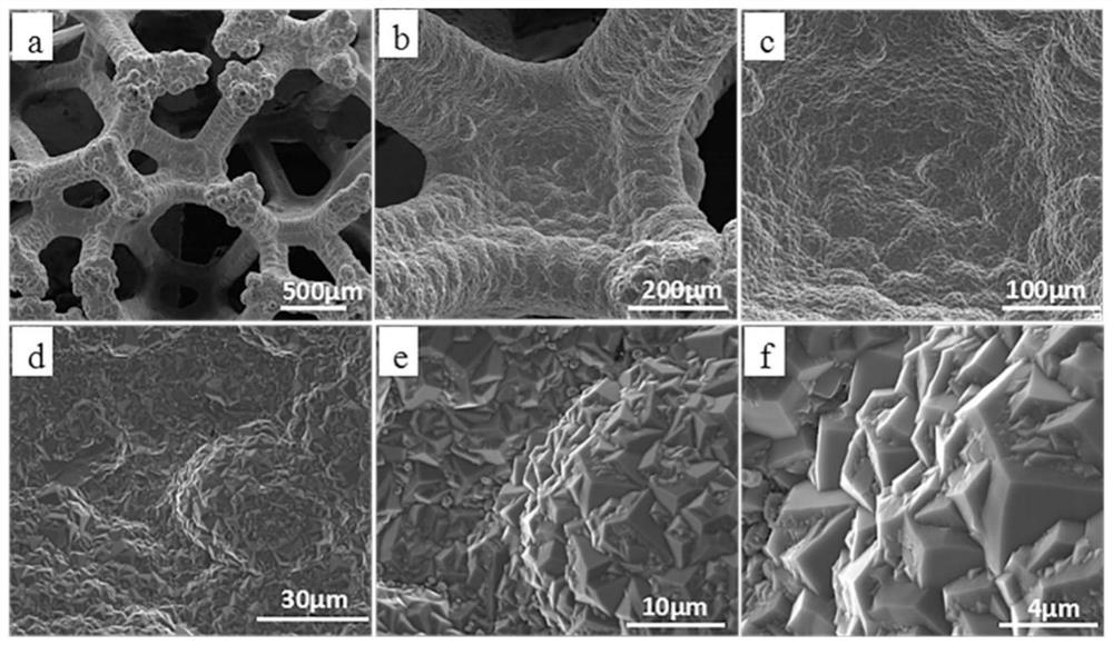
[0071] Example 3: Three-dimensional porous (Al 2 O 3 -Ni composite material)

[0072] (1) Pretreatment of the substrate: ultrasonically clean the surface with acetone and anhydrous ethanol for 10 minutes to remove oil stains and impurities on the surface, immerse it in dilute hydrochloric acid with a mass fraction of 15% for 20 minutes, and obtain micro-etched pits on the surface of the substrate. Ultrasonic cleaning with ethanol for 15min to remove residual acid on the surface;

[0073] (2) Due to the thermal expansion adaptation problem between the substrate surface and the boron-doped diamond layer, in order to facilitate the deposition of boron-doped diamond, a layer of transition layer metal was sputtered on the pretreated substrate surface by a magnetron sputtering method. Titanium Ti layer, adjust sputtering power 80W, deposition time 30min, the thickness of Ti layer is about 10μm;

[0074] (3) Use hot wire CVD to deposit boron-doped diamond film, keep the distance b...


PUM

PropertyMeasurementUnit
thicknessaaaaaaaaaa
quality scoreaaaaaaaaaa

Abstract

The invention discloses a boron-doped diamond electrode with high conductivity, long service life and high specific surface area. The boron-doped diamond electrode uses an etched substrate as an electrode base; or on the surface of an etched substrate After the transition layer is set as the electrode base, a boron-doped diamond layer is set on the surface of the electrode base. The boron-doped diamond layer includes a boron-doped diamond bottom layer with different boron content, a boron-doped diamond middle layer, and a boron-doped diamond layer. Top layer; wherein, the boron-doped diamond bottom layer in contact with the substrate is used as a conductive layer, the boron-doped diamond middle layer is used as a corrosion-resistant layer, the boron-doped diamond top layer is used as a strong electrocatalytic active layer, and the substrate is a metal phase and A composite material composed of ceramic phases, the metal phase is continuously distributed in the composite material; the boron-doped diamond electrode obtained in the present invention has high electrical conductivity, low residual stress, long life, and high specific surface area, and when it is applied to degrade wastewater, the degradation efficiency is greatly improved promote.

Description

technical field [0001] The invention relates to a boron-doped diamond electrode with high conductivity, long life and high specific surface area, a preparation method and application thereof, and belongs to the field of electrode preparation. Background technique [0002] Boron-doped diamond thin film electrodes (BDD) have high mechanical strength, chemical inertness and excellent electrochemical properties, such as wide potential window, high oxygen evolution overpotential and low background current in aqueous solution, Under the same current density, it can efficiently generate hydroxyl radicals, so that organic matter can be quickly removed, the surface has anti-poisoning and anti-pollution capabilities, and can work stably for a long time in strong corrosive media. Even at high electrochemical loads, passing current densities in the range of 2 to 10 A cm 2 After thousands of hours of electrochemical reaction, there is no obvious sign of erosion. The diamond film has hi...

Claims


Application Information

Patent Timeline
Patent Type & Authority Patents(China)
IPC IPC(8): C23C16/27C23C16/02C23C16/56C25B11/052C25B11/053C25B11/083G01N27/327C02F1/461C02F101/30
CPCC23C16/278C23C16/56C23C16/02C23C16/0227C02F1/46109G01N27/327C02F2001/46142C02F2101/30C25B11/051C25B11/091
Inventor 魏秋平马莉周科朝王立峰王宝峰施海平
Owner NANJING DAIMONTE TECH CO LTD
Why Eureka
Try Eureka