
Nanometer welding paste and preparation method and welding method thereof

A technology of nano-welding and nano-copper powder, which is applied in welding media, welding equipment, welding equipment, etc., can solve problems such as welding failure and lower welding quality, and achieve the effects of increased shear strength, improved welding quality, and excellent reliability

Active Publication Date: 2020-09-01
KUNSHAN BRANCH INST OF MICROELECTRONICS OF CHINESE ACADEMY OF SCI
View PDF6 Cites 0 Cited by
  • Summary
  • Abstract
  • Description
  • Claims
  • Application Information

AI Technical Summary

Problems solved by technology

However, when copper and silicon carbide / gallium nitride are soldered, stress will be generated during high temperature application, resulting in soldering failure; at the same time, in the process of soldering with nano-solder paste, it is easy to form voids in the soldering layer, reducing soldering quality

Method used


Image

  • Nanometer welding paste and preparation method and welding method thereof
  • Nanometer welding paste and preparation method and welding method thereof
  • Nanometer welding paste and preparation method and welding method thereof

Examples


preparation example Construction

[0053] The present invention also provides a method for preparing the nano-solder paste described in the above-mentioned technical solution, comprising the following steps:

[0054] a) under protective gas conditions, silicon carbide powder / gallium nitride powder and nano-copper powder are mixed to obtain a mixed powder;

[0055] b) under the condition of protective gas, the obtained mixed powder is mixed with a molding aid to obtain a nano-solder paste.

[0056] Wherein, the types and dosages of the silicon carbide powder / gallium nitride powder, nano-copper powder, and forming aids are consistent with those described in the above technical solution, and will not be repeated here. The present invention has no particular limitation on the type of the protective gas, and it can be an inert gas well known to those skilled in the art, such as nitrogen, helium or argon.

[0057] In the step a), the mixing is preferably high-speed stirring and mixing, and the speed is preferably 50...

Embodiment 1

[0072] 1.1 Preparation of solder paste

[0073] Under the protection of argon, 5 parts of nano-copper powder and 4 parts of silicon carbide powder were stirred and mixed at a high speed at 200 rpm for 10 minutes to obtain a mixed powder.

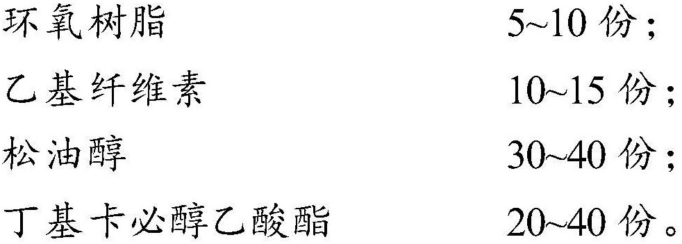
[0074] Mix 7 parts of epoxy resin (the brand is NC-3000), 11 parts of ethyl cellulose, 35 parts of terpineol and 30 parts of butyl carbitol acetate to obtain a molding aid.

[0075] Under the protection of argon, 9 parts of the above mixed powder and 1 part of forming aid were stirred and mixed at a high speed at a speed of 200 rpm for 30 minutes to obtain a nano-solder paste.

[0076] The above preparation process can be found in figure 1 , figure 1 It is a schematic flow chart of the preparation process of the solder paste in Example 1 of the present invention, wherein, figure 1 a is a schematic diagram of raw materials, figure 1 b is a schematic diagram of powder mixing, figure 1 c is a schematic diagram of powder-liquid mixing.

[...

Embodiment 2~4

[0080] Embodiment 2~4, comparative example 1

[0081] 1.1 Preparation of solder paste

[0082] Examples 2-4: The solder paste preparation process of Example 1 was followed, except that the ratio of raw materials was different. For the ratio of raw materials in each embodiment, refer to Table 1.


PUM

PropertyMeasurementUnit
Particle sizeaaaaaaaaaa
Shear strengthaaaaaaaaaa

Abstract

The invention provides nanometer welding paste and a preparation method and a welding method thereof. The nanometer welding paste comprises the following components in percentage by mass of 10-80% ofnano-copper powder, 10-80% of silicon carbide powder / gallium nitride powder and 10-20% of a forming additive, wherein the forming additive comprises a thickening agent and a solvent. In the nanometerwelding paste, the nano-copper powder and the silicon carbide powder / gallium nitride powder are matched in a certain proportion and are solved with the aid of the forming additive to be applied to thewelding of a silicon carbide / gallium nitride test piece, so the shear strength after welding can be improved, the thermal stress mismatch between the test piece and a substrate at high temperature isreduced, and the thermal stability is improved. Meanwhile, the porosity of a welding interface can be effectively reduced, and the welding quality is improved.

Description

technical field [0001] The invention relates to the technical field of power electronics, in particular to a nano solder paste, a preparation method and a welding method thereof. Background technique [0002] With the gradual deepening of research on wide-bandgap semiconductor materials and the continuous development of related preparation technologies, power electronics technology has become one of the key research directions in the world, and it plays an important role in supporting the national economy. In aerospace, automotive electronics , green energy and other fields play a vital role. However, with the development of technology, various application fields have put forward higher requirements for power electronic devices, such as higher operating frequency, higher device power and higher operating temperature, etc., making the packaging and module integration of devices The heat dissipation and reliability have become the main bottleneck of current technology develop...

Claims


Application Information

Patent Timeline
IPC IPC(8): B23K35/30B23K35/362B23K35/02B23K31/02
CPCB23K35/302B23K35/3601B23K35/362B23K35/0255B23K31/02
Inventor 徐杨王英辉
Owner KUNSHAN BRANCH INST OF MICROELECTRONICS OF CHINESE ACADEMY OF SCI
Learn More