Cadmium zinc telluride/silicon gamma ray X-ray detector and preparation method thereof
A detector and gamma ray technology, which is applied in the field of composite cadmium zinc telluride-silicon detector and its preparation, can solve the problems of unsatisfactory detection sensitivity and detection efficiency of the cadmium zinc telluride detector, and achieves the advantages of being suitable for popularization and use, high time efficiency and the like. Resolution, method is simple and easy to implement
- Summary
- Abstract
- Description
- Claims
- Application Information
AI Technical Summary
Problems solved by technology
Method used
Image
Examples
Embodiment 1
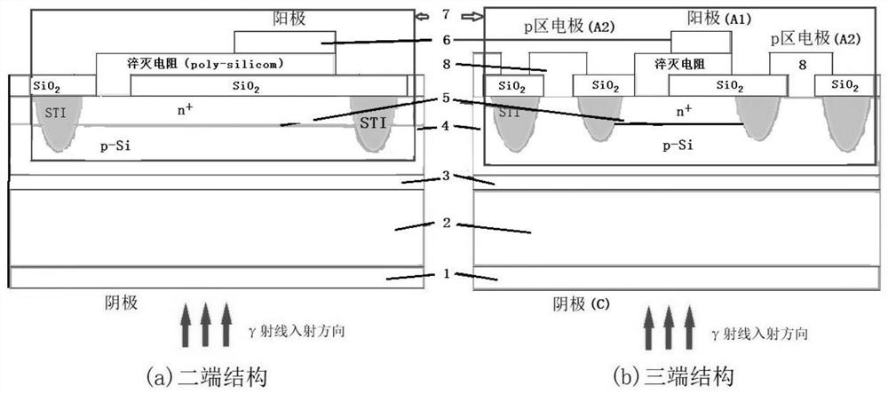
[0030] In this example, see figure 1 , a cadmium zinc telluride / silicon γ-ray X-ray detector, including a ray absorption detection area and a charge multiplication area; the ray absorption detection area is composed of a first metal electrode layer 1, a cadmium zinc telluride wafer 2 and a bonding transition layer 3, The bonding transition layer 3 adopts a metal layer, so that the ray absorption detection area forms a metal-semiconductor-metal structure, wherein the first metal electrode layer 1 is used as a cathode, and the bonding transition layer 3 is used as a bonding interface transition with the silicon wafer 4 layer, thereby the main functional layer structure of the detector is formed by indirect bonding of the CdZnTe wafer 2 and the silicon wafer 4 through the bonding transition layer 3; Composition, the multiplication region on the silicon chip adopts the SiPM unit 7 structure of the silicon photomultiplier tube, the SiPM unit 7 is composed of a silicon wafer 4, an a...
Embodiment 2
[0042] This embodiment is basically the same as Embodiment 1, especially in that:
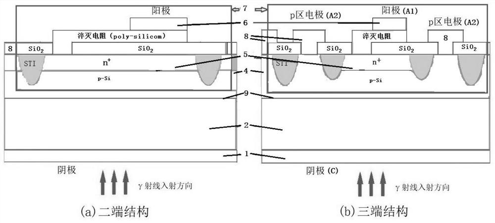
[0043] In this example, see figure 2 , a cadmium zinc telluride / silicon γ-ray X-ray detector, including a ray absorption detection area and a charge multiplication area; the ray absorption detection area is composed of a first metal electrode layer 1, a cadmium zinc telluride wafer 2 and a bonding interface 9, wherein The first metal electrode layer 1 is used as a cathode, thereby forming a composite crystal by direct bonding of the cadmium zinc telluride wafer 2 and the silicon wafer 4, and there is a bonding interface 9 between the cadmium zinc telluride wafer 2 and the silicon wafer 4, forming a detector Main functional layer structure; the charge multiplication area is made up of the avalanche PN junction 5 made on the silicon wafer 4, the multiplication area on the silicon wafer adopts the SiPM unit 7 structure of the silicon photomultiplier tube, and the SiPM unit 7 is composed of the si...
Embodiment 3
[0048] This embodiment is basically the same as the previous embodiment, and the special features are:
[0049] In this embodiment, when preparing a CdZnTe gamma-ray X-ray detector with high detection sensitivity, the surface treatment of the CZT crystal, the preparation of the Si chip and the preparation of the upper electrode of the CZT wafer all adopt the aforementioned process, that is, in the first embodiment a, b, d. The bonding process of CZT wafer and Si wafer is as follows:
[0050] Indirect bonding of CZT wafer and Si sheet: use In as the intermediate transition layer to form a CZT-In-Si transition layer bonding structure, or use graphene as the intermediate transition layer to form a CZT-Gr-Si transition layer bonding structure, Then again in atmosphere or 10 -2 ~10 -5 The vacuum of Pa and the conditions of 25-350°C are used for bonding.
[0051] The cadmium zinc telluride gamma-ray X-ray detector with high detection sensitivity in this embodiment greatly improv...
PUM
| Property | Measurement | Unit |
|---|---|---|
| Particle size | aaaaa | aaaaa |
Abstract
Description
Claims
Application Information

