PBn type InAsSb infrared detector material
A technology of infrared detector and contact layer, which is applied in the direction of semiconductor devices, sustainable manufacturing/processing, electrical components, etc., can solve the problems of low quantum efficiency of devices, excessive recombination current, and high working voltage, so as to suppress the generation of dark current, Effect of improving quantum efficiency and suppressing generation-recombination current
- Summary
- Abstract
- Description
- Claims
- Application Information
AI Technical Summary
Problems solved by technology
Method used
Image
Examples
Embodiment 1
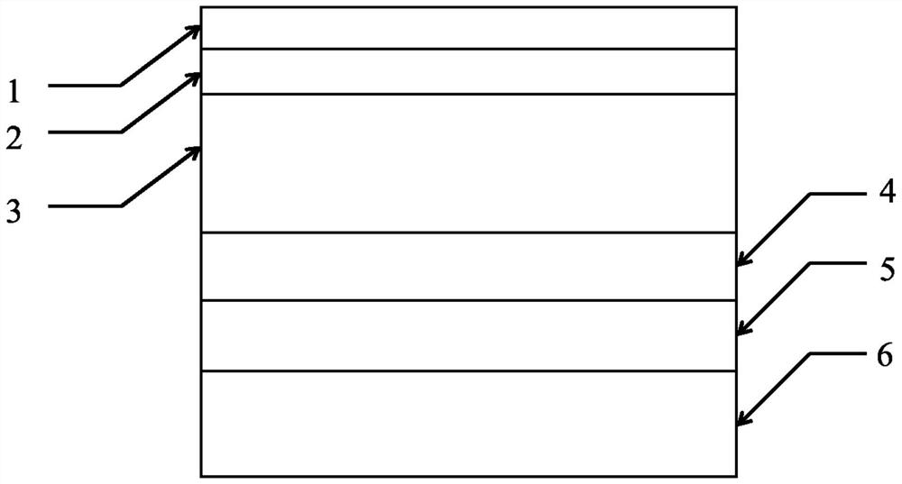
[0031] A kind of PBn type InAsSb infrared detector material, such as figure 1 As shown, the structure of the infrared detector material is top electrode contact layer 1 , barrier layer 2 , absorption layer 3 , bottom electrode contact layer 4 , buffer layer 5 and substrate 6 from top to bottom.
[0032] The material of the top electrode contact layer 1 is p-type gallium antimonide (GaSb) single crystal doped with beryllium (Be); the doping concentration of Be is 1×10 18 cm -3 ; The thickness of the top electrode contact layer 1 is 300nm.
[0033] The material of the barrier layer 2 is p-type AlAs doped with Be 0.08 Sb 0.92 single crystal, the doping concentration of Be is 1×10 16 cm -3 , the forbidden band width of the material of the barrier layer 2 is greater than the forbidden band width of the absorbing layer 3, and the lattice matches the lattice of the material of the absorbing layer 3; the thickness of the barrier layer 2 is 120nm.
[0034] The material of the abs...
Embodiment 2
[0045] A kind of PBn type InAsSb infrared detector material, such as figure 1 As shown, the structure of the infrared detector material is top electrode contact layer 1 , barrier layer 2 , absorption layer 3 , bottom electrode contact layer 4 , buffer layer 5 and substrate 6 from top to bottom.
[0046] The material of the top electrode contact layer 1 is p-type GaSb single crystal doped with Be; the doping concentration of Be is 5×10 17 cm -3 ; The thickness of the top electrode contact layer 1 is 300nm.
[0047] The material of the barrier layer 2 is p-type AlAs doped with Be 0.08 Sb 0.92 single crystal, the doping concentration of Be is 1×10 16 cm -3 , the forbidden band width of the material of the barrier layer 2 is larger than the forbidden band width of the absorbing layer 3, and the lattice matches the lattice of the material of the absorbing layer 3; the thickness of the barrier layer 2 is 150nm.
[0048] The material of the absorbing layer 3 is unintentionally ...
Embodiment 3
[0059] Prepare infrared detector A with the PBn type InAsSb infrared detector material that embodiment 1 makes, prepare infrared detector B with the PBn type InAsSb infrared detector material that makes of embodiment 2, the preparation method of described infrared detector is as follows :
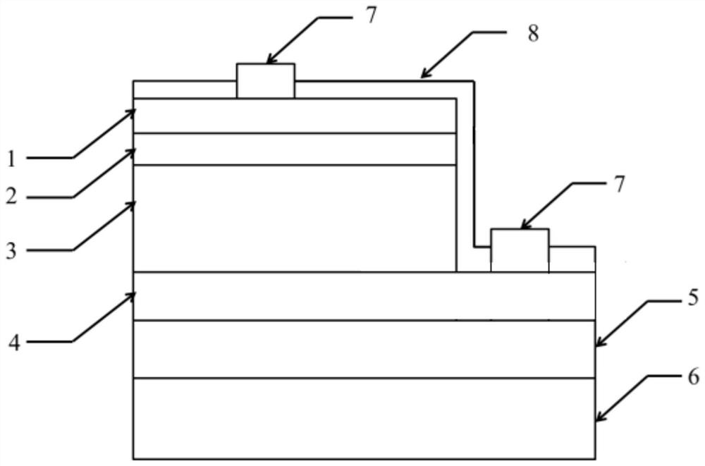
[0060] By combining dry etching and wet etching, first mesa etching the bottom electrode contact layer 4 (as in Example 1 to obtain a mesa height of 3.2 μm) to prepare samples; then using inductively coupled enhanced chemical vapor deposition (ICPCVD ) system sequentially deposits 100 nm thick SiO at 120 °C 2 and 300nm thick Si 3 N 4 Composite film passivates the sample to form a passivation layer 8, wherein SiO 2 Using SiH 4 , O 2 and Ar, the gas flow rate is 6.0sccm, 7.5sccm and 156sccm, respectively, to prepare Si 3 N 4 Using SiH 4 , NH 3 and Ar, the gas flow rates are 6.0sccm, 8sccm and 278sccm, respectively, to physically protect and electrically insulate the sample surface; u...
PUM
| Property | Measurement | Unit |
|---|---|---|
| Thickness | aaaaa | aaaaa |
| Thickness | aaaaa | aaaaa |
| Thickness | aaaaa | aaaaa |
Abstract
Description
Claims
Application Information


