
Blue light OLED based on solvent vapor phase processing hole injection layer and preparation method thereof

A hole injection layer and hole transport layer technology, used in electrical components, semiconductor/solid-state device manufacturing, electrical solid-state devices, etc., can solve problems such as the inability to accurately control the penetration depth of solvents and poor film quality.

Pending Publication Date: 2021-03-16
SHANGHAI UNIV
View PDF5 Cites 3 Cited by
  • Summary
  • Abstract
  • Description
  • Claims
  • Application Information

AI Technical Summary

Problems solved by technology

From the perspective of low cost, repeatability and safety, it is preferable to form a gas-phase atmosphere in a closed container with an appropriate organic solvent or acid to treat the hole injection layer of the blue OLED device, which overcomes the solvent penetration caused by solvent doping or immersion etching Defects where the depth cannot be precisely controlled and poor film quality leads to severe leakage currents

Method used


Image

  • Blue light OLED based on solvent vapor phase processing hole injection layer and preparation method thereof
  • Blue light OLED based on solvent vapor phase processing hole injection layer and preparation method thereof
  • Blue light OLED based on solvent vapor phase processing hole injection layer and preparation method thereof

Examples


Embodiment 1

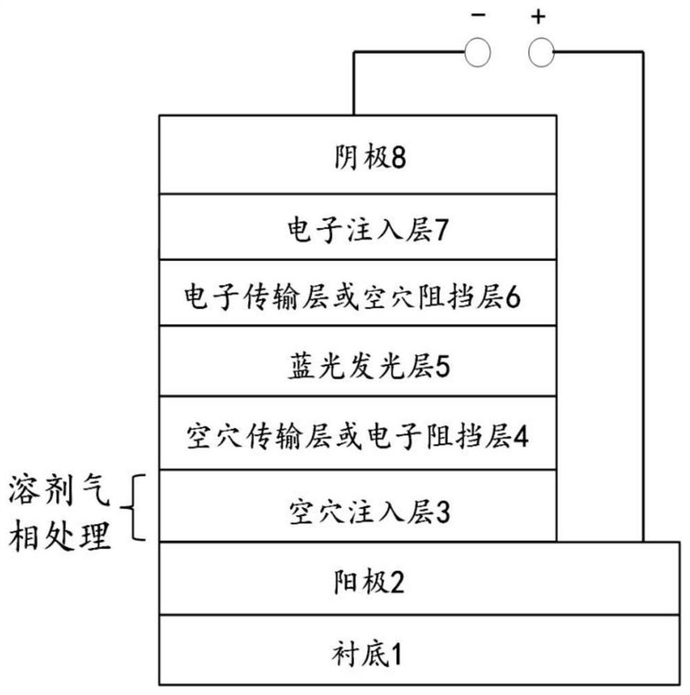
[0050] see figure 1, a blue light OLED based on solvent vapor phase treatment of the hole injection layer, which consists of substrate layer 1, anode layer 2, hole injection layer 3, hole transport layer or electron blocking layer 4, blue light emitting layer 5, The electron transport layer or hole blocking layer 6, the electron injection layer 7 and the conductive cathode layer 8 are combined, and the light-emitting guest material of the blue light-emitting layer adopts fluorescent, phosphorescent or thermally activated delayed fluorescent materials that emit blue light.

[0051] In this embodiment, the blue-light OLED device based on the solvent vapor phase treatment of the hole injection layer has high color stability and reasonable structure. The hole mobility can realize the balance of carrier transport and the improvement of optical coupling in blue OLED at the same time.

Embodiment 2

[0053] This embodiment is basically the same as Embodiment 1, and the special features are as follows:

[0054] In this embodiment, the hole injection layer 3 is made of a polymer material, including at least one of the following materials: poly(3,4-ethylenedioxythiophene)-poly(styrenesulfonate), poly[N,N'-bis(4-butylphenyl) -N,N'-bis(phenyl)-benzidine], poly[bis(4-phenyl)(2,4,6-trimethylphenyl)amine], poly[(9,9-dioctylfluorenyl-2,7-diyl)- co-(4,4'-(N-(4-sec-butylphenyl)diphenylamine)](TFB);

[0055] In this embodiment, or the hole injection layer 3 adopts organic small molecule materials, including at least one of the following materials: 4,4',4"-tris(N-3-methylphenyl-N-phenyl-amino)triphenylamine, 4,4',4"-tris(N-(naphthalen-2-yl)-N-phenyl-amino)triphenylamine, copper(II)phthalocyanine(CuPC), titanium(IV)oxidephthalocyanine, pyrazino[2,3-f ][1,10]phenanthroline-2,3-dicarbonitrile, N,N,N',N'-tetrakis(4-methoxyphenyl)benzidine, N,N'-diphenyl-N,N'-di-[4-( N,N-di-p-tolyl-amino...

Embodiment 3

[0065] In this embodiment, a method for preparing a blue-light OLED based on solvent vapor phase treatment of a hole injection layer includes the following preparation steps:

[0066] 1) The substrate and the anode are cleaned and dried with nitrogen;

[0067] 2) Prepare a hole injection layer on the surface of the anode by using spin coating, printing, spray coating or evaporation, and using a hole injection layer material;

[0068] 3) Solvent vapor phase treatment of the hole injection layer:

[0069] Heat the preferred solvent in a closed container to generate a high-concentration vapor atmosphere, and adjust the flow rate of the solvent gas, put the hole injection layer film in the container and let it stand for a certain period of time, then take it out, and select different annealing temperatures according to the solvent used. Film annealing and drying;

[0070] 4) Using spin coating, printing, spray coating or vapor deposition, on the surface of the hole injection lay...


PUM

PropertyMeasurementUnit
Thicknessaaaaaaaaaa
Thicknessaaaaaaaaaa
Brightnessaaaaaaaaaa

Abstract

The invention discloses a blue light OLED based on a solvent vapor phase processing hole injection layer and a preparation method thereof, and the method comprises the steps: carrying out spin coating, printing, spraying or evaporation of a polymer, small molecule or oxide hole injection layer film with a proper thickness on an anode by employing a solvent vapor phase processing method; placing the film in a high-concentration organic solvent or acid vapor atmosphere, and standing for a certain period of time; and taking out the film, annealing and drying, and sequentially laminating a spin-coating or evaporation hole transport layer or electron blocking layer, a blue light emitting layer, an electron transport layer or hole blocking layer, an electron injection layer and a cathode to obtain a complete blue light OLED device. According to the method provided by the invention, the defect of serious current leakage caused by solvent doping or soaking etching of a hole injection layer isovercome. A scattering structure and phase separation which are beneficial to light emission are formed on the surface of a thin film by utilizing the relatively mild micro-etching effect of gas molecules, so that the optical coupling and external quantum efficiency of the blue-light OLED are remarkably improved.

Description

technical field [0001] The invention relates to the technical field of organic light-emitting diodes, in particular to a blue-light OLED based on a solvent gas-phase treatment of a hole injection layer and a preparation method thereof. Background technique [0002] Organic light-emitting diodes (organic light-emitting diodes, blue OLEDs) have shown great application potential in the fields of full-color flat panel displays and solid-state lighting due to their advantages such as self-illumination, wide viewing angle, rich colors, and low-voltage DC drive. In addition, due to the low power consumption, wide color gamut, fast response, light weight, and mechanical flexibility brought by organic soft materials and flexible substrates, flexible blue OLEDs are highlighting their importance in the field of wearable display and lighting. At present, blue OLEDs have been commercialized in small-size displays. [0003] However, studies have found that in addition to the absolute qua...

Claims


Application Information

Patent Timeline
IPC IPC(8): H01L51/50H01L51/52H01L51/56
CPCH10K50/17H10K50/854H10K71/00
Inventor 郑燕琼唐杰李维光陈俊聪
Owner SHANGHAI UNIV
Learn More