Preparation method of high-quality film lithium niobate micro-nano grating
A lithium niobate, high-quality technology, applied in the directions of light guides, optics, optical components, etc., can solve the problems of reducing the coupling efficiency of gratings and fibers, reducing the etching rate of lithium niobate, and tilting the sidewalls of the grating waveguides. degree and verticality, reduce the difficulty of the process, and reduce the effect of the splicing error
- Summary
- Abstract
- Description
- Claims
- Application Information
AI Technical Summary
Problems solved by technology
Method used
Image
Examples
preparation example Construction
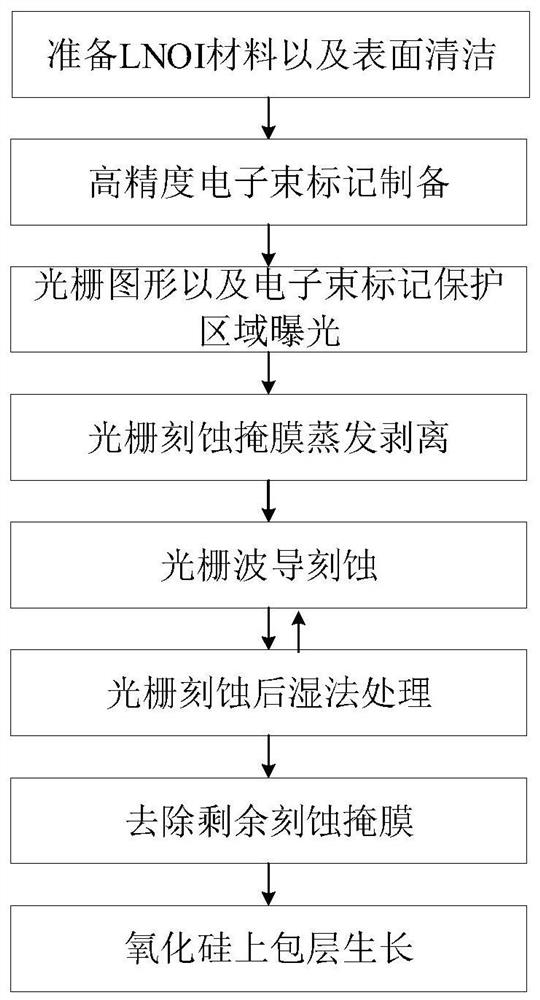
[0020] The invention provides a method for preparing a high-quality thin-film lithium niobate micro-nano grating. The preparation process of the method is shown in figure 1 , including the following steps:
[0021] Step 1, cleaning the surface of the LNOI material;
[0022] Step 2, preparing high-precision electron beam marking;
[0023] Step 3, coating electron beam positive resist ZEP 520A, performing LNOI grating pattern and electron beam marking protection area exposure;
[0024] Step 4, evaporating and stripping Ni metal as a grating waveguide etching mask;
[0025] Step 5, using F-based RIE dry etching and NH 4 OH:H 2 o 2 :H 2 Wet treatment of O, cycled several times to reach the specified etching depth;
[0026] Step 6, using 30% HNO 3 Remove the remaining Ni mask;
[0027] Step 7, growing a silicon oxide upper cladding layer.
[0028] Further, in the step 1, the LNOI material is silicon, silicon dioxide and lithium niobate film.
[0029] Further, in step 1, ...
Embodiment 1
[0040] This embodiment provides a method for preparing a high-quality thin-film lithium niobate grating, which specifically includes the following steps:
[0041] Step 1: Surface cleaning and heat treatment of LNOI material. Specifically, 10 minutes of sonication with acetone, 10 minutes of sonication with ethanol, rinsing with deionized water, drying with nitrogen, and oven drying at 90°C for 15 minutes.
[0042] Step 2: E-beam marking preparation. Spin-coat electron beam positive colloid UV 135 at a speed of 3000rpm / min. After spin-coating, put it on a hot plate at 130℃ and bake for 90s. Electron beam evaporates Ti / Pt alloy with a thickness of 20 / 80nm. After evaporation, soak in acetone for 1 For more than an hour, remove the metal on the film, then replace it with acetone and sonicate for 10 minutes, ethanol for 10 minutes, and finally wash with deionized water and dry in an oven at 90°C for 20 minutes.
[0043] Step 3: E-beam mark protection and raster pattern exposure. ...
PUM
| Property | Measurement | Unit |
|---|---|---|
| thickness | aaaaa | aaaaa |
| thickness | aaaaa | aaaaa |
| thickness | aaaaa | aaaaa |
Abstract
Description
Claims
Application Information


