Deep ultraviolet semiconductor light emitting diode epitaxial structure

A technology of light-emitting diodes and epitaxial structures, which is applied to semiconductor devices, electrical components, circuits, etc., can solve the problems of reducing the internal quantum efficiency of deep ultraviolet LEDs, and cannot effectively improve the light extraction efficiency of deep ultraviolet LEDs, so as to improve light extraction efficiency, Effects of improved light extraction efficiency and increased growth height

Active Publication Date: 2021-04-09
HEBEI UNIV OF TECH
View PDF5 Cites 1 Cited by
  • Summary
  • Abstract
  • Description
  • Claims
  • Application Information

AI Technical Summary

Problems solved by technology

When these air cones merge, a large number of dislocations will be generated due to different crystal orientations, and these dislocations will directly extend into the quantum well, thereby reducing the internal quantum efficiency (IQE) of the deep ultraviolet LED.
In addition, usually AlGaN-based deep ultraviolet LEDs use pGaN as the hole transport layer and ohmic contact layer, which has a large amount of light absorption. Although PSS introduces scattering centers, most of the light emitted above these scattering centers is scattered first. For pGaN, most of it is absorbed by pGaN, which cannot effectively improve the light extraction efficiency of deep ultraviolet LEDs

Method used


Image

  • Deep ultraviolet semiconductor light emitting diode epitaxial structure
  • Deep ultraviolet semiconductor light emitting diode epitaxial structure
  • Deep ultraviolet semiconductor light emitting diode epitaxial structure

Examples


Embodiment 1

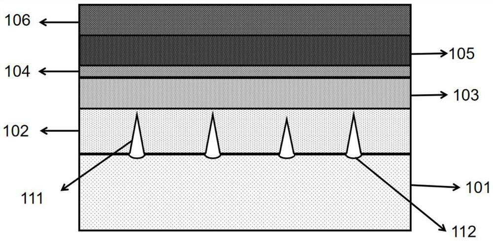
[0048]The epitaxial structure of the DUV LED of the present embodiment, such asfigure 2 As shown, the pattern substrate 101, the semiconductor buffer layer 102, the n-type semiconductor material layer 103, the n-type semiconductor material layer 103, the multi-quantum well layer 104, the P-type electron blocking layer 105, the P-type semiconductor material Transport layer 106;

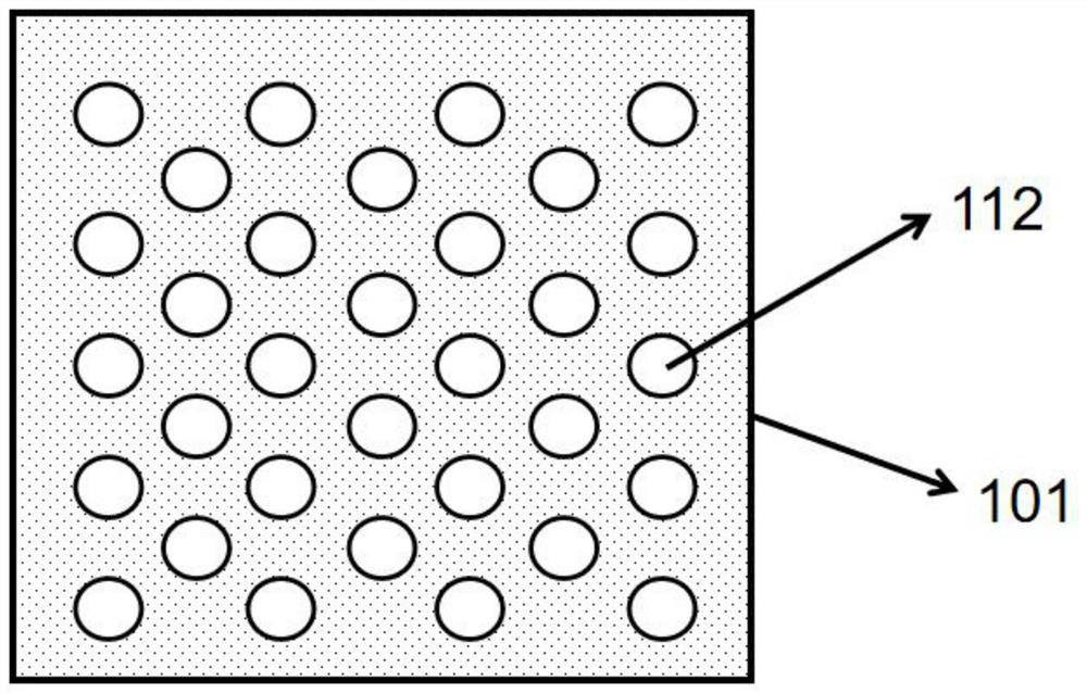
[0049]The graphic substrate, such asimage 3 As shown, the graphic substrate 101 etching the recess 112, the groove 112 is a pit, between 500 nm to 550 nm, and the depth is between 250 nm to 300 nm, and the groove 112 is on the graphic substrate 101. The graph is arranged, and the present embodiment is the rectangular square array (egimage 3 As shown), the spacing is 20 μm.

[0050]Among them, each groove 112 on the surface of the graphic substrate 101 is grown having a cavity structure, the cavity structure passes through the semiconductor buffer layer 102, the n-type semiconductor material layer 103, the multi-qu...

Embodiment 2

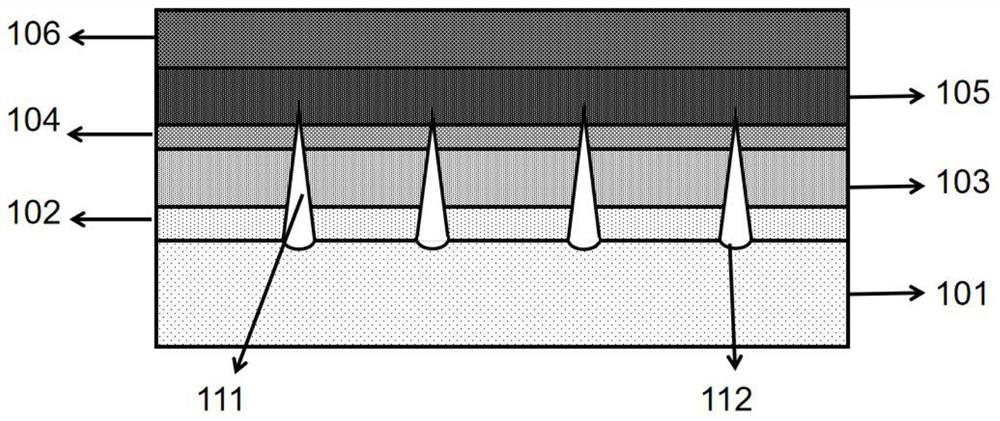
[0065]Other steps are in Example 1, and different in the substrate graphic size of the substrate etched on the substrate by nano-embossed or holographic photolithography techniques, between 2 to 4 μm, and the depth is between 1 to 2 μm. This allows the cavity to pass through the entire epitaxial structure, such asFigure 6As shown, that is, the cavity is in an unacceptable state when the epitaxial structure is completed.

[0066]Further, the substrate pattern can also be arranged in an annular radiation, and the arrangement spacing is 2 to 200 μm; the substrate pattern can be a rectangular strip, or other irregular geometry, the area is 0.25 ~ 400 μm.2The substrate may be aluminum nitride, gallium nitride, 4H-SiC, aluminum oxide single crystal, gallium oxide, 6H-SiC, and the like.


PUM

PropertyMeasurementUnit
sizeaaaaaaaaaa
sizeaaaaaaaaaa
depthaaaaaaaaaa

Abstract

The invention relates to a deep ultraviolet semiconductor light emitting diode epitaxial structure. The epitaxial structure sequentially comprises a patterned substrate, a semiconductor buffer layer, an n-type semiconductor material layer, a multi-quantum well layer, a p-type electron blocking layer and a p-type semiconductor material transmission layer in an epitaxial direction, wherein grooves are etched in the patterned substrate, a cavity structure vertically grows upwards on each groove, and the cavity structures penetrate through the semiconductor buffer layer, the n-type semiconductor material layer and the multi-quantum well layer. The top part positions of the cavity structures are divided into the following three types: the first type is that the cavity structures are polymerized on the p-type electron barrier layer, and the polymerization depth of the cavities in the p-type electron barrier layer is 10-100 nm; or the second type is that the cavity structures continuously penetrate through the p-type electron barrier layer and are polymerized on the p-type semiconductor material transmission layer, and the polymerization depth of the cavities in the p-type semiconductor material transmission layer is 10-500 nm; or the third type is that cavity structures continuously penetrate through the p-type electron barrier layer and the p-type semiconductor material transmission layer, cavities are not polymerized, and round holes appear in the surface of the p-type semiconductor material transmission layer. According to the deep ultraviolet semiconductor light emitting diode epitaxial structure, the internal quantum efficiency of the deep ultraviolet LED can be improved; and the cavity structures are incorporated into quantum wells, so that the scattering feature of light can be effectively improved, and the light extraction efficiency of the deep ultraviolet light-emitting diode is improved.

Description

Technical field[0001]The technical solution of the present invention relates to a semiconductor device, and is specifically a deep ultraviolet semiconductor light emitting diode and a preparation method thereof.Background technique[0002]Deep ultraviolet light refers to ultraviolet light having a wavelength of less than 300 nm. Due to the short wavelength, there is a great development potential in the fields of sensing, medical, disinfection, light curing, and water purification. Deep Uvorared Light Diode (DUV LED) is a light-emitting diode that can emit deep-ultraviolet light, compared to traditional mercury lamps, which has a series of advantages long, low operating voltage, smart and non-toxic environmental protection, so Wide attention from all walks of life. The AlGan-based DUV LED is a DUV LED with AlGaN as P-N, which is also the most common DUV LED.[0003]Conventional Algan-based DUV LEDs are grown on sapphire substrate, because sapphire has high lightweight and more mature LED...

Claims


Application Information

Patent Timeline
Patent Type & Authority Applications(China)
IPC IPC(8): H01L33/20H01L33/24H01L33/06H01L33/14H01L33/32H01L33/00
CPCH01L33/007H01L33/06H01L33/14H01L33/145H01L33/20H01L33/24H01L33/32
Inventor 张勇辉张沐垚张紫辉
Owner HEBEI UNIV OF TECH
Why Eureka
Try Eureka