Flexible broadband uncooled infrared detector and preparation method thereof
An uncooled infrared and wide-band technology, applied in the field of infrared detectors, can solve the problems of restricting the application of intelligent electronic systems, fixed shape, rigid structure, etc., and achieve the effects of light weight, reduced manufacturing cost, and high shock resistance
- Summary
- Abstract
- Description
- Claims
- Application Information
AI Technical Summary
Problems solved by technology
Method used
Image
Examples
Embodiment 1
[0047] 1. Prepare a sodium chloride sacrificial layer on a silicon wafer by thermal evaporation, with a thickness of 500 nm.
[0048] 2. On the sacrificial layer of sodium chloride, a polyimide support layer was prepared by solution spin coating, with a thickness of 1 μm.
[0049] 3. Manganese-cobalt-nickel-oxygen thermistor film was prepared on the polyimide support layer by magnetron sputtering method, with a thickness of 6 μm.
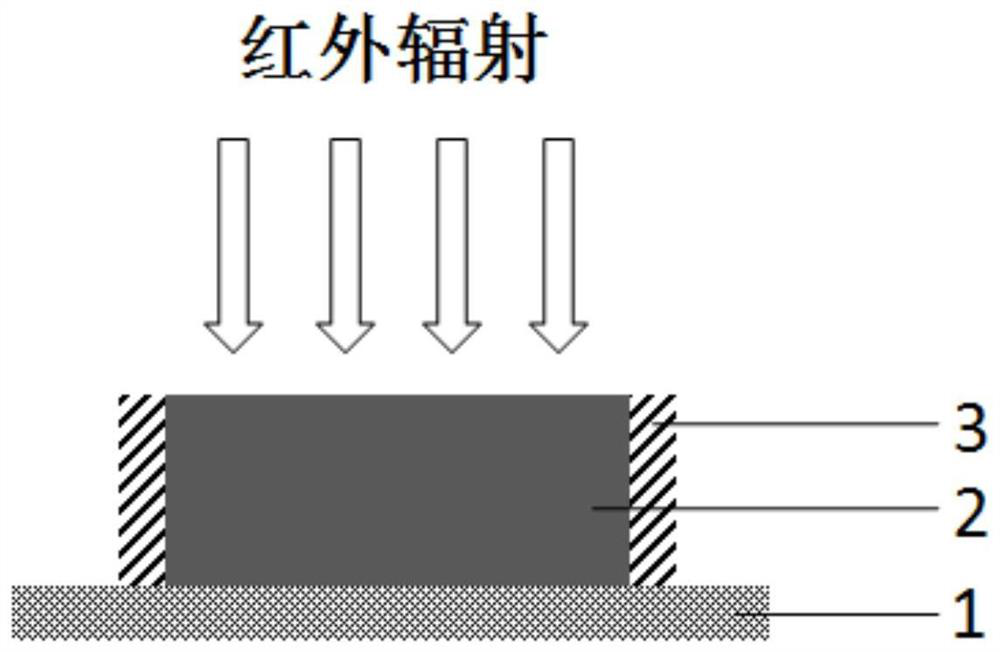
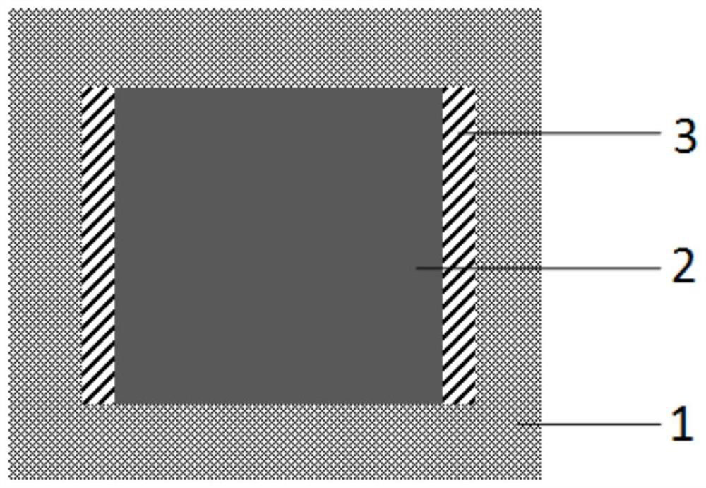
[0050] 4. Manganese-cobalt-nickel-oxygen thin-film detection elements are prepared on the manganese-cobalt-nickel-oxygen thermistor film through photolithography, corrosion, development and other photolithographic patterning processes. The area of the detection element is 30 μm×30 μm.
[0051] 5. Through photolithography, corrosion, development and other photolithographic patterning processes, the dual ion beam sputtering method is used to prepare chromium and gold composite electrodes at both ends of the manganese-cobalt-nickel-oxygen thin film d...
Embodiment 2
[0054] 1. Prepare a sacrificial layer of sodium chloride on a silicon wafer by thermal evaporation, with a thickness of 700nm.
[0055] 2. On the sacrificial layer of sodium chloride, a polyimide support layer was prepared by solution spin coating, with a thickness of 1.5 μm.
[0056] 3. Manganese-cobalt-nickel-oxygen thermistor film was prepared on the polyimide support layer by magnetron sputtering method, with a thickness of 8 μm.
[0057] 4. Manganese-cobalt-nickel-oxygen thin-film detection elements are prepared on the manganese-cobalt-nickel-oxygen thermistor film through photolithography, corrosion, development and other photolithographic patterning processes. The area of the detection element is 50 μm×50 μm.
[0058] 5. Through photolithography, corrosion, development and other photolithographic patterning processes, the dual ion beam sputtering method is used to prepare chromium and gold composite electrodes at both ends of the manganese-cobalt-nickel-oxygen thin fi...
Embodiment 3
[0061] 1. Prepare a sodium chloride sacrificial layer on a silicon wafer by thermal evaporation, with a thickness of 800 nm.
[0062] 2. On the sacrificial layer of sodium chloride, a polyimide support layer was prepared by solution spin coating, with a thickness of 2 μm.
[0063] 3. Manganese-cobalt-nickel-oxygen thermistor film was prepared on the polyimide support layer by magnetron sputtering method, with a thickness of 9 μm.
[0064] 4. Manganese-cobalt-nickel-oxygen thin-film detection elements are prepared on the manganese-cobalt-nickel-oxygen thermistor film through photolithography, corrosion, development and other photolithographic patterning processes. The area of the detection element is 75 μm×75 μm.
[0065] 5. Through photolithography, corrosion, development and other photolithographic patterning processes, the magnetron sputtering method is used to prepare chromium and gold composite electrodes at both ends of the manganese-cobalt-nickel-oxygen thin film detec...
PUM
| Property | Measurement | Unit |
|---|---|---|
| Thickness | aaaaa | aaaaa |
| Thickness | aaaaa | aaaaa |
| Thickness | aaaaa | aaaaa |
Abstract
Description
Claims
Application Information


