

Nanometer soldering flux, preparation method thereof, device and welding method
A welding method and nano-welding technology, applied in welding equipment, welding medium, welding/cutting medium/material, etc., can solve the problem of easy oxidation of nano-flux
- Summary
- Abstract
- Description
- Claims
- Application Information
AI Technical Summary
Problems solved by technology
Method used
Image

Examples
preparation example Construction
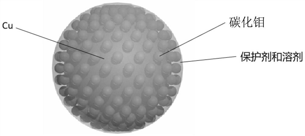
[0055] The embodiment of the present invention also provides a preparation method of nano-flux, comprising the following steps:
[0056] Mixing the protective agent, the nanomolybdenum carbide, and the solvent to obtain an antioxidant dispersion;
[0057] The nano copper powder is mixed with the anti-oxidation dispersion liquid to obtain a copper molybdenum carbide mixture.
[0058] In some embodiments, before mixing the copper powder with the anti-oxidation dispersion, a step of removing oxides on the surface of the nano-copper powder is included. The nano-copper powder can be surface-treated by ethanol containing organic acid or inorganic acid to obtain the surface-treated nano-copper powder. Preferably, the organic acid can be selected from one or more of acetic acid, oxalic acid, malonic acid, glutaric acid, lactic acid, citric acid, and the inorganic acid is one or more of dilute hydrochloric acid, dilute sulfuric acid and dilute nitric acid. Various.
[0059] In some ...
Embodiment 1
[0075] This example provides a Mo that can resist oxidation storage 2 The preparation method of C-nanometer copper flux, comprises the following steps:
[0076] Preparation of anti-oxidant dispersion: polyvinylpyrrolidone (protective agent) and ethanol (solvent) are mixed with Mo with a particle size of 6nm in a mass ratio of 1:10 2 C powder was ultrasonically mixed for 20 minutes to obtain an antioxidant dispersion. Among them, nano Mo 2 C powder is Mo prepared by temperature-rising reduction method. 2 C powder, accounting for the whole Mo 2 C - 1% of the mass of nano-copper flux; polyvinylpyrrolidone and ethanol account for the overall Mo 2 C - 19% of the mass of nano copper solder.
[0077] Surface treatment of nano-copper powder: Prepare nano-copper powder with a particle size of 40nm by polyol method, and configure 30g / L ethanol solution of citric acid.
[0078] The nano-copper powder was added into the prepared citric acid ethanol solution and subjected to ultrason...
Embodiment 2
[0081]This example provides a Mo that can resist oxidation storage 2 The preparation method of C-nanometer copper flux, comprises the following steps:
[0082] Preparation of anti-oxidant dispersion: polyvinylpyrrolidone (protective agent) and ethanol (solvent) are mixed with Mo with a particle size of 6nm in a mass ratio of 1:10 2 C powder was ultrasonically mixed for 20 minutes to obtain an antioxidant dispersion. Among them, nano Mo 2 C powder is Mo prepared by temperature-rising reduction method. 2 C powder, accounting for the whole Mo 2 C - 3% of the mass of nano copper flux; polyvinylpyrrolidone and ethanol account for the overall Mo 2 C - 17% of the mass of nano-copper flux.
[0083] Surface treatment of nano-copper powder: Prepare nano-copper powder with a particle size of 40nm by polyol method, and configure 30g / L ethanol solution of citric acid.
[0084] The nano-copper powder was added into the prepared citric acid ethanol solution and subjected to ultrasonic ...
PUM
| Property | Measurement | Unit |
|---|---|---|
| Particle size | aaaaa | aaaaa |
| Particle size | aaaaa | aaaaa |
| Thickness | aaaaa | aaaaa |
Abstract
Description
Claims
Application Information