
A preparation method of SERS substrate based on 2D noble metal nanostructure

A nanostructure and noble metal technology, applied in metal material coating process, instrument, vacuum evaporation plating, etc., can solve the problems that it is difficult to prepare a plasma nanostructure array, and it is difficult to evenly distribute hot spots, so as to improve the detection sensitivity , excellent repeatability and stability, good periodic effect

Active Publication Date: 2022-03-15
UNIV OF ELECTRONICS SCI & TECH OF CHINA
View PDF6 Cites 0 Cited by
  • Summary
  • Abstract
  • Description
  • Claims
  • Application Information

AI Technical Summary

Problems solved by technology

For extremely low concentrations of target molecules, it is difficult to evenly distribute on these sparse and unevenly distributed hotspots, and practical SERS detection requires point-to-point and batch-to-batch reproducibility
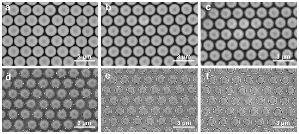
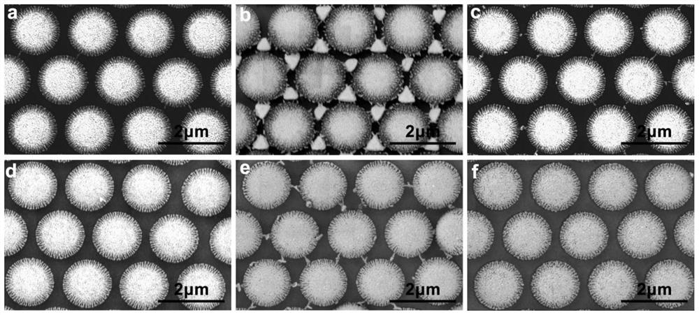
Moreover, it is difficult to prepare closely arranged arrays of plasmonic nanostructures with sub-20 nanometer gaps on the surface of colloidal particles only by colloidal self-assembly technology.

Method used


Image

  • A preparation method of SERS substrate based on 2D noble metal nanostructure
  • A preparation method of SERS substrate based on 2D noble metal nanostructure
  • A preparation method of SERS substrate based on 2D noble metal nanostructure

Examples


Embodiment 1

[0034] This embodiment provides a method for processing a SERS substrate based on a 2D noble metal nanostructure, which specifically includes the following steps:

[0035] S1, the surface is deposited with 300nm silicon oxide single crystal silicon (referred to as SiO 2 / Si) The substrate is successively placed in acetone, absolute ethanol and deionized water for ultrasonic cleaning for 10 minutes, taken out and dried with nitrogen, and treated with an ultraviolet ozone system for 30 minutes to make the surface of the substrate exhibit superhydrophilic properties;

[0036]S2. Using the colloidal self-assembly method to self-assemble a layer of polystyrene (PS) microsphere arrays in a regular and orderly arrangement on the surface of the substrate after step S1, and then place the substrate in a drying oven at 60°C for drying treatment 90min, and then further increase the temperature to 80°C for 5min heat treatment to obtain substrate A;

[0037] In the step S2, the specific s...

Embodiment 2

[0046] This embodiment provides a method for processing a SERS substrate based on a 2D noble metal nanostructure, which specifically includes the following steps:

[0047] S1, put 2 pieces of SiO 2 The / Si substrate was placed in acetone, absolute ethanol, and deionized water for 8 minutes to be ultrasonically cleaned, taken out and dried with nitrogen, and then treated with an ultraviolet ozone system for 25 minutes to make the surface of the substrate appear super-hydrophilic;

[0048] S2. Using the colloidal self-assembly method to self-assemble a layer of polystyrene (PS) microsphere arrays in a regular and orderly arrangement on the surface of the substrate after step S1, and then place the substrate in a drying oven at 60°C for drying treatment After 60 minutes, the temperature was further raised to 80°C for 5 minutes of heat treatment to obtain substrate A;

[0049] S3, using a plasma etching machine to carry out oxygen plasma etching on the substrate A prepared in ste...


PUM

PropertyMeasurementUnit
diameteraaaaaaaaaa
porosityaaaaaaaaaa
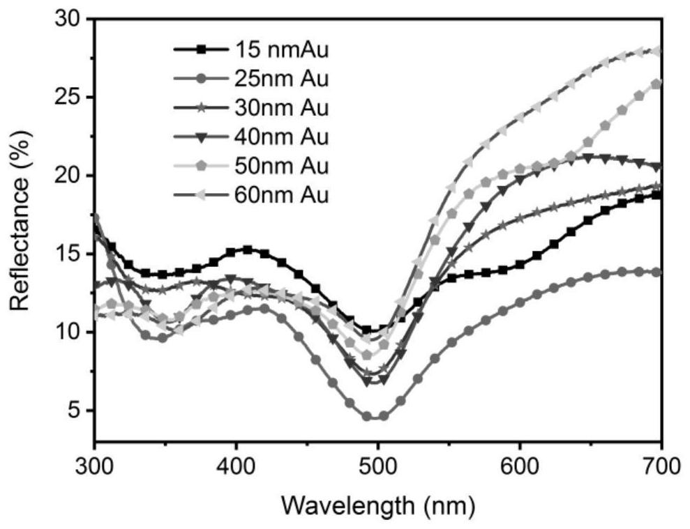
reflectanceaaaaaaaaaa

Abstract

The invention provides a method for preparing a SERS substrate based on a 2D noble metal nanostructure, belonging to the technical field of nanoprocessing. Specifically: first self-assemble a layer of polymer microsphere array on the surface of the substrate, after oxygen plasma etching, the polymer microsphere array with a smooth surface becomes a plush polymer microsphere array, and use this structure as a template in the Precious metals are deposited on the surface, and the SERS substrate is obtained after etching away the template. The surface of the SERS substrate is covered with a noble metal layer with needle-like protrusion structures, the gap between the needle-like protrusion structures is less than 20nm, the nanostructures are densely arranged, evenly distributed, and have good periodicity, which is conducive to obtaining a continuous and uniform enhanced electromagnetic field, significantly The detection sensitivity of the SERS device is improved, and it has excellent repeatability and stability. In addition, the preparation method provided by the invention can also realize high-efficiency processing and large-scale production, and reduce production costs.

Description

technical field [0001] The invention belongs to the technical field of nano-processing, and in particular relates to a preparation method of a SERS substrate based on a 2D noble metal nanostructure. Background technique [0002] Surface-enhanced Raman scattering (SERS) is one of the most impressive applications of plasmonic physics and is crucial for understanding various fundamental interfacial processes and interaction mechanisms. SERS enhances the local electromagnetic (EM) energy to 6 or more orders of magnitude through diverse metal nanogap (so-called hotspots), greatly enhancing the intermolecular and molecule-metal interactions, thus enabling single-molecule detection and Identify, and collect rich vibrational information with sub-nanometer precision. Commonly used SERS substrates include gold nanoparticles (AuNPs) arrays, silver nanoparticles (AgNPs) arrays, etc. Although gaps below 10 nm can be easily prepared on these substrates as enhancement units, the repeatabi...

Claims


Application Information

Patent Timeline
Patent Type & Authority Patents(China)
IPC IPC(8): C23C14/24C23C14/30C23C14/18C23C14/20C23C14/04G01N21/65
CPCC23C14/24C23C14/30C23C14/18C23C14/20C23C14/042G01N21/658
Inventor 熊杰汪红波杜新川雷天宇陈伟晏超贻王显福
Owner UNIV OF ELECTRONICS SCI & TECH OF CHINA
Learn More