
Patsnap Eureka
For R&D, Patsnap Eureka makes reading and utilizing patents & technical documents easy.
Patsnap Eureka AIR
Designed for self-driven R&D workflows. Generate viable solutions, solve complex R&D challenges, empower your innovation with AI.

Patsnap Eureka Materials
Designed for material experts only. Revolutionize your material R&D, from search, analyze, to developing new materials.

TechResearch
Generate reliable direction feasibility study reports for your R&D in just a few steps.

TechSeek
Discover and master advanced knowledge NOW. Basics, ideas, possibilities, all at once.

TechMind
As an expert in R&D Theories, TechMind can generates customized viable solutions instantly.

TechRisk
Analyze your overall solution with one click, know your potential R&D risks in advance.

TechMonitor
Get weekly tech updates, stay abreast of the latest tech innovations and key insights.
Antimony selenide thin film with high (hk1) crystal face abundance, antimony selenide thin film solar cell and preparation method of antimony selenide thin film solar cell
A technology of solar cells and antimony selenide, which is applied in circuits, photovoltaic power generation, electrical components, etc., can solve the problems of low efficiency and poor stability of antimony selenide thin-film solar cells, and is suitable for industrial production and application, and improves the crystal surface Abundance, the effect of reducing jumping between bands
- Summary
- Abstract
- Description
- Claims
- Application Information
AI Technical Summary
Problems solved by technology
Method used
Image

Examples
Embodiment 1
[0051] The specific preparation method of antimony selenide thin film solar cell is as follows:
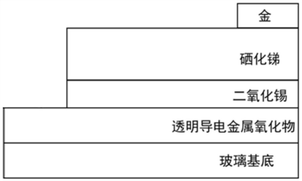
[0052] 1) Use the existing deposition method to plate an ITO layer with a thickness of 150nm on the surface of the glass substrate or directly purchase a glass substrate coated with an ITO layer as the substrate;
[0053] 2) cleaning step 1) glass substrate coated with an ITO layer;
[0054] Use acetone, absolute ethanol, and deionized water to ultrasonically clean them in an ultrasonic cleaning machine for 20 minutes. Before changing the solvent, rinse with deionized water to remove the residue of the original solvent, and then clean the substrate with high pressure. Blow dry with nitrogen gas and place in a container covered with dust-free paper.
[0055] 3) Deposit SnO on the surface of the transparent conductive metal oxide layer by magnetron sputtering 2 The buffer layer;
[0056] 3.1) Fix the substrate cleaned in step 2) on the sample stage, put it into a vacuum chamber, ...
Embodiment 2
[0070] The difference with Example 1 is limited to: after the growth of the antimony selenide thin film in step 4), the antimony selenide thin film is cooled to room temperature with the furnace, the chamber is opened to take out the growth source of antimony selenide, the selenium source is put in, and the chamber is closed to draw Vacuum to 5 Pa, and then both the upper heating stage and the lower heating stage are heated to 350° C. for selenization annealing. The annealing time is 30 minutes, that is, the selenization annealing is performed on the antimony selenide thin film.
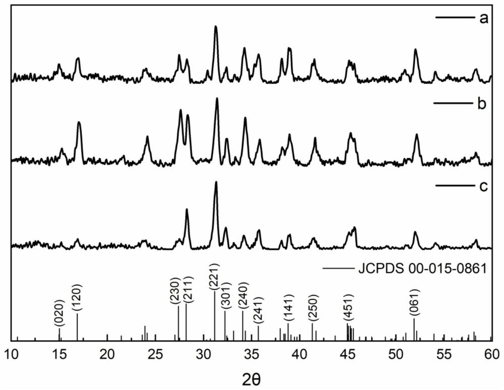
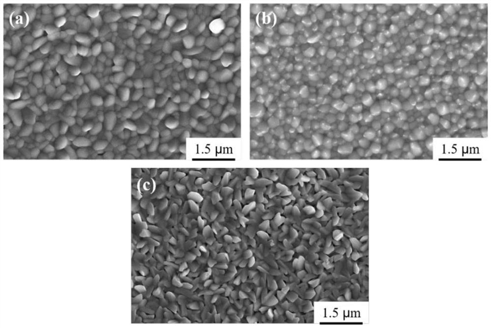
[0071] This embodiment has carried out selenization annealing to the grown antimony selenide thin film, and the X-ray diffraction pattern of antimony selenide thin film is shown in figure 2 In (c), SEM picture see image 3 In (b), the J-V spectrum of the antimony selenide thin film solar cell is shown in Figure 4 (c) in.
Embodiment 3
[0073] The difference from Example 1 is only: After the growth of the antimony selenide thin film in step 4), the temperature in the sublimation furnace chamber is lowered to room temperature, and then the temperature is raised to 350°C for in-situ annealing. The annealing time is 30 min, that is, the The antimony selenide film was annealed in situ.
[0074] In this embodiment, in-situ annealing is performed on the grown antimony selenide thin film, and the X-ray diffraction pattern of the antimony selenide thin film is shown in figure 2 In (b), SEM picture see image 3 In (a), the J-V spectrum of the antimony selenide thin film solar cell is shown in Figure 4 (b) in.
[0075] Embodiment 1~Example 3 can be seen, as image 3 Comparison of SEM surface morphology of antimony selenide thin film. It can be seen that the grain shape is sharper before annealing and there are a small amount of pores between the grains. These pores will hinder the transport of carriers and reduce ...
PUM
| Property | Measurement | Unit |
|---|---|---|
| thickness | aaaaa | aaaaa |
| thickness | aaaaa | aaaaa |
| thickness | aaaaa | aaaaa |
Abstract
Description
Claims
Application Information
 - R&D Engineer
- R&D Manager
- IP Professional
- Industry Leading Data Capabilities
- Powerful AI technology
- Patent DNA Extraction
Browse by: Latest US Patents, China's latest patents, Technical Efficacy Thesaurus, Application Domain, Technology Topic, Popular Technical Reports.
© 2024 PatSnap. All rights reserved.Legal|Privacy policy|Modern Slavery Act Transparency Statement|Sitemap|About US| Contact US: help@patsnap.com