
A method for making an interlayer cross-wire connection structure and a circuit board

A technology of connection structure and production method, which is applied in the direction of mechanically removing conductive materials, printed circuit, printed circuit manufacturing, etc., can solve the problems of blocked vias, high production cost, low production efficiency, etc. Small footprint and high production efficiency

Active Publication Date: 2022-07-22
SIHUI FUJI ELECTRONICS TECH
View PDF10 Cites 0 Cited by
  • Summary
  • Abstract
  • Description
  • Claims
  • Application Information

AI Technical Summary

Problems solved by technology

[0004] The circuit layers in the circuit board are connected by a via hole. The via hole is a metallized hole that conducts electricity in the circuit board. The via hole and the annular ring occupy more space on the circuit board. For conventional circuit boards In general, there are more areas that can be used to make holes and annular rings, but it will also affect the precise layout of the circuit. At the same time, for IC substrates with a relatively small area, there is not so much area that can be used. up
[0005] During the production process of the circuit board, the deviation of the hole relative to the annular ring will be caused by the deviation of the drilling, the deformation of the film, and the positioning deviation. The annular ring needs to be more than 4mil to ensure that the hole will not break out of the annular ring. Breaking out of the hole ring will cause the hole copper to be corroded and the via hole will be blocked, so the circular drilling method is no longer suitable for the development needs of the IC substrate; the conventional mechanical drilling connection method has an aperture size of 300 micron, single-side annular ring is 100 micron, and line width is 100 micron, then the area occupied by the conventional hole connection method is 196250 square microns. Smudge, substrate cracks and damage, etc., the reliability of the hole connection is not high; even if the laser drilling method is used, the hole diameter for the IC substrate is generally 100 microns, and the hole ring on one side is 50 microns. The area occupied by the hole is also 31400 microns
[0006] The wiring technology of traditional electronic circuits is mainly based on the subtractive method and semi-additive method, while both SAP (semi-additive method) and m-SAP (improved SAP method) need to use chemical copper, flash etching, electroplating, micro-etching, etc. Wet technology, the use of chemical etching method will inevitably have the problem of side erosion, the size of the side erosion is closely related to the thickness of the copper, and the thickness of the bottom copper is less than 12μm, and it will be difficult to manufacture and press the copper foil; and to increase The bonding force between the copper foil and the base material adopts the method of roughening the surface of the copper foil and the surface of the resin, which will increase the processing cost, and the roughened surface will have a bad influence on the transmission of the signal; the above process steps also have complex procedures, High energy consumption, high cost and serious environmental pollution
[0007] In addition, because the thickness of copper on the surface of the printed circuit board is generally required to be greater than 25 microns, at the same time, affected by factors such as the uniformity of electroplating copper, the development accuracy of the dry film, the alignment exposure accuracy, the uniformity of etching, and side etching, traditional printing The wire width and the spacing between wires obtained by the manufacturing method of the circuit board circuit are generally controlled above 30 μm / 30 μm (line width / spacing), and as the line width and line spacing are smaller and the density is higher, the production cost of the product is higher. The lower the pass rate, it is difficult to produce ultra-precision circuits with line width / spacing less than 30μm / 30μm, such as ultra-high-density circuits such as 20μm / 20μm, 10μm / 10μm, etc. It is difficult to manufacture more precise circuits using traditional methods However, the method of printing with high-performance conductive nano-conductive ink has the problems of difficult material preparation and extremely low production efficiency

Method used


Image

  • A method for making an interlayer cross-wire connection structure and a circuit board

Examples


Embodiment 1

[0053] The manufacturing method of an interlayer cross-wire connection structure shown in this embodiment sequentially includes the following processing steps:

[0054] (1) Material cutting: prepare an insulating base material with a size of 500*600 mm and a thickness of 25 μm, and the insulating base material is a polyimide film (ie, a PI film).

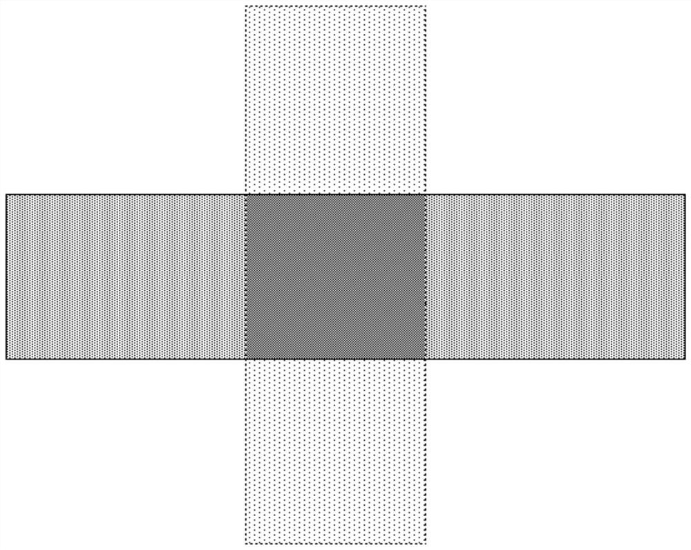
[0055] (2) Laser scribing: A 355-nanometer UV laser is used to ablate the first connecting line groove with a depth of 15 μm on the first surface of the insulating substrate, and the length of the first connecting line groove is 0.1 mm and the width is 20 μm ; In other specific embodiments, the depth of the first connecting wire slot can also be set to be ≥ 1 / 2 of the thickness of the insulating base material and less than the thickness of the insulating base material.

[0056] (3) Laser grooving: According to the circuit pattern required by the design, a first circuit groove with a depth of 10 μm is ablated on the first surface of ...

Embodiment 2

[0069] The manufacturing method of an interlayer cross-wire connection structure shown in this embodiment is basically the same as the manufacturing method described in Embodiment 1, except that the following steps are further included after step (8):

[0070] (9) Grinding plate: After the nickel is deposited, the plate surface is smoothed by the grinding plate, so that the surface of the precision circuit is flush with the surface of the insulating substrate.

Embodiment 3

[0072] The manufacturing method of an interlayer cross-wire connection structure shown in this embodiment sequentially includes the following processing steps:

[0073] (1) Material cutting: prepare a PI film with a size of 500*600mm and a thickness of 25μm and an inner core board with the same length and width. The inner core board is a double-sided copper clad core board, and the middle core board is The thickness of the dielectric layer is 0.15mm.

[0074] (2) Making the inner layer circuit: The inner layer circuit is made on the two surfaces of the inner layer core board by the negative film process.

[0075] (3) Film: paste PI film on both surfaces of the inner core board to form a production board.

[0076](4) Laser scribing: a 355-nanometer UV laser is used to ablate the first connecting line groove on the first surface of the production board. The length of the first connecting line groove is 0.1 mm, the width is 20 μm, and the depth is greater than 0.1 mm. 0.075mm+2...


PUM


Abstract

The invention discloses a manufacturing method and a circuit board of an interlayer cross-wire connection structure. The manufacturing method comprises the following steps: manufacturing a first connecting wire slot and a first circuit connected to each other on a first surface of an insulating base material The groove is made on the second surface of the insulating base material to connect the second connecting wire groove and the second circuit groove. The depth of the first and second connecting wire grooves is ≥ 1 / 2 of the thickness of the insulating base material. The depth of the second line groove is less than 1 / 2 of the thickness of the insulating base material; the first and second connecting line grooves are crossed to form a through hole in the overlapping area of ​​the two connecting line grooves; The copper layer on the surface is removed from the board; then a layer of nickel is deposited by immersion nickel, and the surface of the circuit is flattened by grinding to obtain a precision circuit. The invention adopts the method of laser ablating two intersecting wire grooves and forming through holes in the overlapping area of ​​the two intersecting wire grooves, so that the area occupied by the through holes connected between the layers is greatly reduced, and is suitable for the interlayer of the IC carrier board. connect.

Description

technical field [0001] The invention relates to the technical field of printed circuit board fabrication, in particular to a fabrication method of an interlayer cross-wire connection structure and a circuit board. Background technique [0002] The 21st century has entered a highly information-based society, and the demand for information consumption is becoming more and more vigorous. High-speed, high-performance and light, thin and short are the mainstream development trends of future electronic products. Microelectronic packaging technology is also developing rapidly. The application of thin and higher packaging density devices is increasing, which makes the circuit board as a supporting platform for electronic components to change to the direction of high density, high integration and miniaturization; therefore, the wiring density of circuit boards is becoming more and more precise, The line width and spacing are gradually developing towards micron-level ultra-precision. ...

Claims


Application Information

Patent Timeline
Patent Type & Authority Patents(China)
IPC IPC(8): H05K3/10H05K3/00H05K3/04H05K3/42H05K3/24
CPCH05K3/108H05K3/0026H05K3/04H05K3/429H05K3/24H05K2203/107H05K2203/025
Inventor 黄明安温淦尹李轩
Owner SIHUI FUJI ELECTRONICS TECH
Learn More