Chemical method for promoting silver nanowire nodes to be welded into continuous low-resistance conductive network

A nano-silver wire, conductive network technology, applied in nanotechnology, nanotechnology, liquid chemical plating and other directions, can solve the problems of large contact resistance and contact stability, damage, limited resistance reduction, etc., to increase the bonding strength. and overlap area, increase the contact area, reduce the effect of contact resistance

Pending Publication Date: 2021-07-13
重庆烯宇新材料科技有限公司
View PDF11 Cites 2 Cited by
  • Summary
  • Abstract
  • Description
  • Claims
  • Application Information

AI Technical Summary

Problems solved by technology

[0002] As optoelectronic equipment tends to be miniaturized, sophisticated and high-performance, making it a foldable and portable product, the requirements for the quality of transparent conductive films are getting higher and higher, and the requirements for the film preparation process are also increasing. Although transparent conductive films have many outstanding advantages, how to obtain low sheet resistance under high light transmittance is still a challenge, which is an urgent problem to be solved. The conductivity of AgNWs network obviously depends on the AgNWs. The AgNWs network prepared by the traditional method has large contact resistance and contact stability problems, which is not conducive to the fine application of electronic equipment. The conductivity of the AgNWs network obviously depends on the connection between AgNWs. Equipped with a grid structure for excellent electrical conductivity
[0003] However, traditional methods such as high-temperature annealing welding, plasma welding, Joule heat welding, and high-temperature hot pressing will cause varying degrees of damage to plastic substrate materials with low glass transition temperatures, affecting the stability and flexibility of TCFs. Sex, and high optical power density will greatly limit the application in mass production
[0004] The light welding method disclosed in CN109727704A, i.e. photon sintering, can reduce the node resistance value of nano-silver wire to a certain extent, improve the flexibility of TCFs and the adhesiveness of silver wire and base material, but the resistance value reduces very limited (photon The resistance after sintering is >70Ωsq-1 at 550nm), and its effect is far from meeting the technical requirements of large-size touch screens (<30Ωsq-1 at 550nm), and photovoltaic welding equipment is expensive, and large-scale production and technology in the field of large-scale There is an obvious bottleneck in the application
[0005] Although the disclosed method of CN111112862A does not involve a weak reducing agent, the implementation conditions are gentle and wide, but the effect is very limited, and the resistance value of the conductive film only reduces by about 20% after being processed by the method disclosed by this patent, which is far from meeting the needs of large sizes (more than 55 inches). The high-sensitivity requirements of flexible touch displays indicate that the contact resistance of the overlapping points of the nano-silver wires cannot be effectively reduced.
[0006] CN105568270B and CN105702381B use chemical welding solution to soak or dip-coat the plastic substrate and nano-silver wire coating, which can strengthen the nano-silver wire superposition and local welding to reduce the resistance of the conductive film, but the preparation of the chemical plating solution is too cumbersome and will use There is still a long way to go to concentrated nitric acid and industrial mass production applications
[0007] The methods of CN105575477B and CN109735833A involve freshly preparing an electroless plating solution containing silver source and reducing agent to infiltrate the nano-silver wire transparent conductive film, and the square resistance is obviously reduced, but optical properties such as light transmittance and haze are sacrificed. Large-scale touch screens have reached mass production applications, and further improvements are needed
[0008] In addition, the methods disclosed in the above patents do not solve the adhesion and adhesion between the nano-silver wire network and the substrate quality inspection, resulting in the performance stability and life of TCFs cannot be guaranteed.

Method used


Image

  • Chemical method for promoting silver nanowire nodes to be welded into continuous low-resistance conductive network
  • Chemical method for promoting silver nanowire nodes to be welded into continuous low-resistance conductive network
  • Chemical method for promoting silver nanowire nodes to be welded into continuous low-resistance conductive network

Examples


Embodiment 1

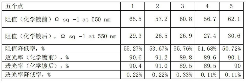
[0049] see figure 2 , the flexible transparent PET film (thickness 125 μm) that is coated with nano silver wire is immersed in the silver ammonia solution containing 30mM glucose, silver source concentration 35mM, immersion time 2min; After cleaning the conductive film with pure water, place the flexible transparent PET film coated with nano-silver wire in a drying device for drying, and the drying stability should not exceed 110°C, which ensures the drying of the flexible transparent PET film coated with nano-silver wire security at the time.

[0050] After the drying is completed, take 5 points, use a four-corner probe to detect the resistance value and light transmittance of each point before and after electroless plating treatment, and list the data changes before and after treatment as follows figure 1 .

Embodiment 2

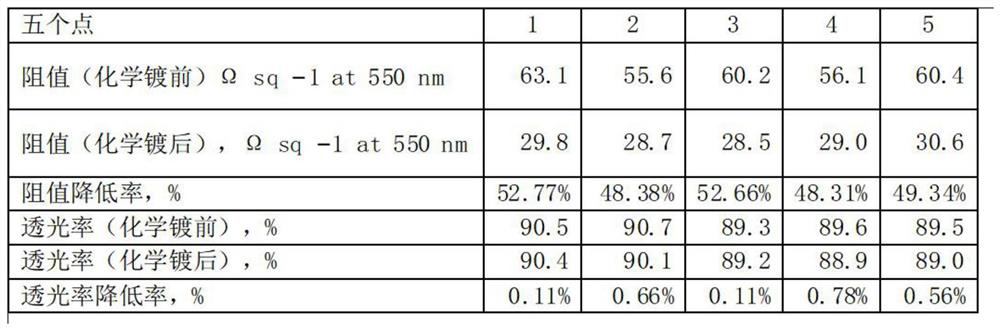
[0052] see image 3 , the flexible transparent PEN film (thickness 200 μ m) that is coated with nano-silver wire is immersed in the silver ammonia solution containing 50mM ascorbic acid, the concentration of silver source is 50mM, and soaking time is 3min; Clean the conductive film with pure water, and then place the flexible transparent PET film coated with nano-silver wire in a drying device for drying, and the drying stability should not exceed 110°C, ensuring that the flexible transparent PET film coated with nano-silver wire is dry security.

[0053] Take 5 points, use a four-corner probe to detect the resistance value and light transmittance of each point before and after electroless plating treatment, and list the data changes before and after treatment as follows figure 2 :

Embodiment 3

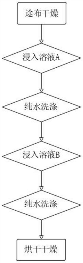
[0055] see Figure 4 , immerse the flexible transparent PI film (thickness 100 μm) coated with nano-silver wire in the silver ammonia solution containing 60mM isoascorbic acid, the silver source concentration is 45mM, and the soaking time is 4min; after washing with pure water, immerse in 150mM NaF aqueous solution for 8 minutes , clean the conductive film with pure water, and then place the flexible transparent PET film coated with nano-silver wire in a drying device for drying, and the drying stability should not exceed 110°C, which ensures the drying of the flexible transparent PET film coated with nano-silver wire security at the time.

[0056] Take 5 points, use a four-corner probe to detect the resistance value and light transmittance of each point before and after electroless plating treatment, and list the data changes before and after treatment as follows image 3 .


PUM


Abstract

The invention discloses a chemical method for promoting silver nanowire nodes to be welded into a continuous low-resistance conductive network. The construction process comprises the steps of coating, curing and drying, soaking in a solution A, washing with pure water, soaking in a solution B, washing with pure water, and drying. The solution comprises the following main components by mass: the solution A: a silver ammonia solution or silver salt such as silver nitrate, a reducing agent (glucose, ascorbic acid and the like) and an alkaline additive; and the solution B: a halogen salt solution such as a sodium fluoride (NaF) aqueous solution. Six steps are comprised. According to the method disclosed by the invention, the resistance value of the TCFs can be reduced by more than 50%, the light transmittance of the TCFs is not obviously changed in the whole process, and the requirement of a large-size flexible touch screen on high touch sensitivity can be met; the method is simple and easy to implement, expensive equipment for physical hot pressing, plasma treatment, light irradiation treatment and the like does not need to be added, and an environment-unfriendly reagent is not involved, so that the method is time-saving, efficient, wide and mild in conditions, economical, applicable and suitable for industrial large-scale production.

Description

technical field [0001] The invention relates to the technical field of nano-silver wire spot welding, in particular to a chemical method for promoting the welding of nano-silver wire nodes into a continuous low-resistance conductive network. Background technique [0002] As optoelectronic equipment tends to be miniaturized, sophisticated and high-performance, making it a foldable and portable product, the requirements for the quality of transparent conductive films are getting higher and higher, and the requirements for the film preparation process are also increasing. Although transparent conductive films have many outstanding advantages, how to obtain low sheet resistance under high light transmittance is still a challenge, which is an urgent problem to be solved. The conductivity of AgNWs network obviously depends on the AgNWs. The AgNWs network prepared by the traditional method has large contact resistance and contact stability problems, which is not conducive to the fi...

Claims


Application Information

Patent Timeline
Patent Type & Authority Applications(China)
IPC IPC(8): C23C18/44B82Y30/00B82Y40/00
CPCC23C18/44B82Y30/00B82Y40/00
Inventor 甘李杨棚竣周明杨建文唐波
Owner 重庆烯宇新材料科技有限公司
Why Eureka
Try Eureka