Black silicon manufacturing method based on mechanical grinding auxiliary corrosion

A technology of mechanical grinding and manufacturing methods, which is applied in semiconductor/solid-state device manufacturing, electrical components, circuits, etc., and can solve problems such as degraded device performance, low black silicon production capacity, and poor near-infrared absorption enhancement effect

Pending Publication Date: 2021-09-10
THE 44TH INST OF CHINA ELECTRONICS TECH GROUP CORP
View PDF10 Cites 0 Cited by
  • Summary
  • Abstract
  • Description
  • Claims
  • Application Information

AI Technical Summary

Problems solved by technology

The femtosecond laser scanning method uses femtosecond laser pulses to act on the surface of the silicon wafer to obtain a needle-shaped or columnar black silicon structure, which has the advantages of good black silicon shape and good infrared absorption enhancement effect, but this method also has the disadvantages of expensive equipment, Black silicon has the disadvantages of extremely low production capacity and large lattice damage; metal ion assisted wet chemical etching, using Au + 、Pt + , Mn + 、Ni + 、Cu + Plasma-assisted wet etching forms pyramids or hole-shaped black silicon, which has the advantages of simple equipment and low production cost, but it is easy to cause metal ion contamination and greatly degrade device performance; maskless dry etching uses the crystal orientation of plasma itself Selective etching and micro-mask to form a columnar black silicon structure has the advantage of simple process, but there are problems such as poor inter-chip / intra-chip uniformity and poor process repeatability; nanoimprinting generally adopts nanoimprinting on silicon wafers first. Form a black silicon micro-nano structure mask on the surface, and then use dry etching to transfer the mask pattern to the silicon substrate to form a black silicon structure. This method has the advantages of good uniformity and designable structure, but it also has the advantages of high cost and close Infrared absorption enhancement effect is poor (nanoimprinted black silicon microstructure is shallow, otherwise the microstructure cannot be molded during nanoimprinting) and other shortcomings

Method used


Image

  • Black silicon manufacturing method based on mechanical grinding auxiliary corrosion
  • Black silicon manufacturing method based on mechanical grinding auxiliary corrosion
  • Black silicon manufacturing method based on mechanical grinding auxiliary corrosion

Examples


Embodiment 1

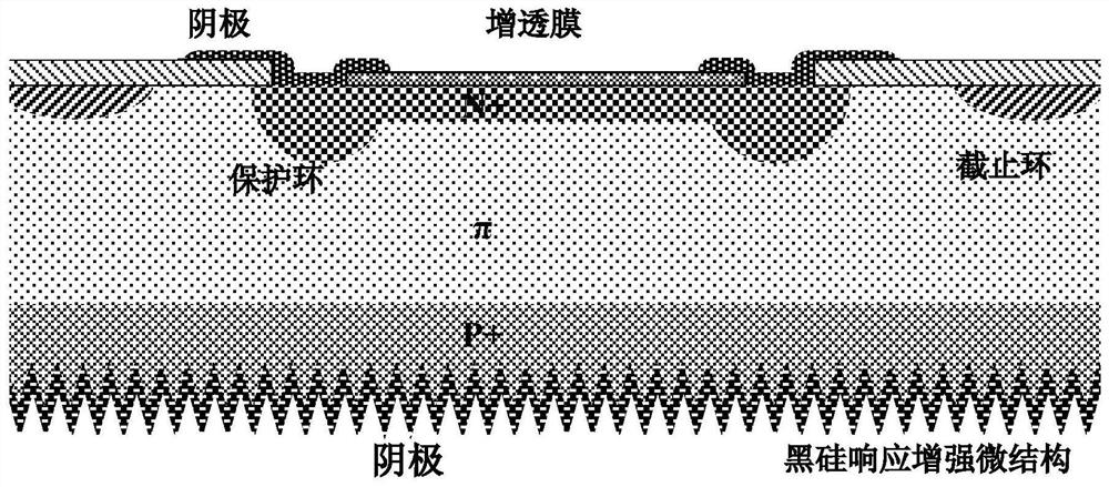
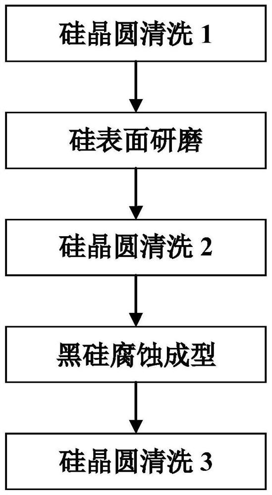
[0036] S0. Complete the fabrication of the front side process of the PIN / APD detector silicon wafer.

[0037] S1. Using an organic cleaning process to clean the wafer to remove surface contamination.

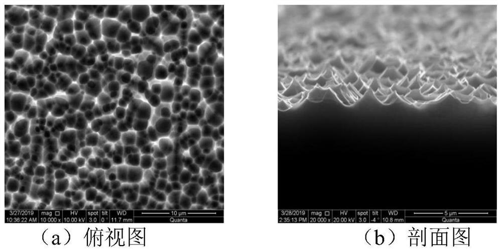
[0038] S2. Use a thinning pad containing corundum (diameter of corundum 0.5 μm ~ 9 μm) and a polishing solution (pH value 10 ~ 12) containing SiO2 abrasive (particle diameter 0.07 μm ~ 1 μm) to assist, and use a mechanical grinding process to process the back of the silicon wafer , produce rough surface and micro-damage on the back of the silicon wafer;

[0039] S3. Using an organic cleaning process to clean the silicon wafer;

[0040] S4, adopt the mixed liquor that comprises phosphoric acid, nitric acid, sulfuric acid and hydrofluoric acid, proportioning is (10%~25%): (20%~50%): (5%~25%): (1%~30%) ), etch the back of the silicon wafer to prepare a black silicon microstructure;

[0041] S5. Using an organic cleaning process to clean the silicon wafer to complete the preparat...


PUM

PropertyMeasurementUnit
diameteraaaaaaaaaa
diameteraaaaaaaaaa

Abstract

The invention relates to the technical field of photoelectric detector preparation, in particular to a black silicon manufacturing method based on mechanical grinding auxiliary corrosion. The method comprises the following steps of: cleaning a silicon wafer, carrying out pretreatment on the surface of the silicon wafer by adopting a mechanical grinding process under the assistance of a thinning pad containing carborundum and a grinding liquid containing a SiO2 grinding material to generate a rough surface and micro-damage on the surface of the silicon wafer, cleaning the surface of the silicon wafer, preparing a black silicon microstructure on the surface of the silicon wafer by using a mixed solution containing nitric acid, hydrofluoric acid, phosphoric acid and sulfuric acid through a wet etching process, and cleaning the silicon wafer, and completing black silicon preparation. According to the invention, the method adopts mechanical grinding to form micro-damage and rough surfaces to assist in wet etching to prepare black silicon, and has the advantages of good near-infrared absorption effect, low dark current, simple process, good uniformity, convenience in batch production, low cost, good process compatibility with silicon photoelectric devices and the like.

Description

technical field [0001] The invention relates to the technical field of photodetector preparation, in particular to a method for manufacturing black silicon based on mechanical grinding and assisted etching. Background technique [0002] Silicon photodetectors (PIN / APD) have the advantages of small dark current, high sensitivity, and low cost, and have been widely used in optical fiber communication, laser ranging, three-dimensional imaging, laser guidance and other fields. In order to further improve system performance and expand the application range, silicon photodetectors are also required to have high responsivity in the near-infrared band (800-1100nm). Black silicon has both micro-nano structure light-trapping effect and photocurrent internal multiplication effect, and can maintain a high absorption rate (≥80%) in the spectral range of 800-1700nm, which is the most important factor for improving the near-infrared responsivity of silicon photodetectors. Methods. [000...

Claims


Application Information

Patent Timeline
Patent Type & Authority Applications(China)
IPC IPC(8): H01L21/02H01L21/306
CPCH01L21/02019H01L21/30604H01L21/02008H01L21/02041
Inventor 黄建江海波鄢真真雷仁方钟玉杰李睿智
Owner THE 44TH INST OF CHINA ELECTRONICS TECH GROUP CORP
Why Eureka
Try Eureka