An organic single crystal heterojunction composite film, its preparation method and application

A technology of heterojunction and composite film, which is applied in the direction of single crystal growth, single crystal growth, chemical instruments and methods, etc., can solve the problems of high energy consumption and high production cost, and achieve simplified preparation process, improved performance and regular shape Effect

Active Publication Date: 2022-01-04
ZHEJIANG UNIV
View PDF4 Cites 0 Cited by
  • Summary
  • Abstract
  • Description
  • Claims
  • Application Information

AI Technical Summary

Problems solved by technology

Chinese patent (CN108342779A) discloses a growth method of a single crystal microribbon p-n heterojunction array, which requires the pre-preparation of a precisely patterned substrate, high energy consumption and high production costs
Existing technologies cannot break through the above barriers

Method used


Image

  • An organic single crystal heterojunction composite film, its preparation method and application
  • An organic single crystal heterojunction composite film, its preparation method and application
  • An organic single crystal heterojunction composite film, its preparation method and application

Examples


Embodiment 1

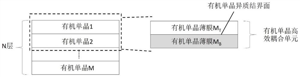
[0097] A compound based on 2,8-difluoro-5,11-bis[2-(triethylsilyl)ethynyl]-anthracendithiophene (Dif-tes-adt) and 6,13-bis(triisopropane An organic single-crystal heterojunction composite film of 5,7,12,14-tetraazapentacene (Tips-tap) and an organic field-effect transistor based on the composite film, including The following steps:

[0098] (1) with heavily doped p + -Si / SiO 2 The substrate is the gate / gate insulating layer, where SiO 2 The thickness of the substrate is 300nm, and a 10nm thick cross-linked polystyrene (c-PS) is spin-coated on the substrate as a substrate modification layer;

[0099] (2) A single p-type semiconductor molecule Dif-tes-adt and an n-type semiconductor molecule Tips-tap were grown on the substrate deposited with Ag nanowires with a diameter of 40nm, and the shape of the organic single crystal film was judged under an optical microscope. Whether the appearance changes significantly when crossing the Ag nanowires, judge the growth interface types...

Embodiment 2

[0109] A compound based on 2,8-difluoro-5,11-bis[2-(triethylsilyl)ethynyl]-anthracendithiophene (Dif-tes-adt) and 6,13-bis(triisopropane An organic single-crystal heterojunction composite film of 5,7,12,14-tetraazapentacene (Tips-tap) and an organic field-effect transistor based on the composite film.

[0110] Refer to Example 1 for the preparation method of the field effect transistor device in Example 2, and the formula and process parameters are shown in Table 1 and Table 2. The morphology, structure and performance characterization methods are the same as those in Example 1. The obtained organic single crystal heterojunction morphology parameters are shown in Table 3. The obtained device properties are shown in Table 4.

Embodiment 3

[0112] A compound based on 2,8-difluoro-5,11-bis[2-(triethylsilyl)ethynyl]-anthracendithiophene (Dif-tes-adt) and 6,13-bis(triisopropane An organic single-crystal heterojunction composite film of 5,7,12,14-tetraazapentacene (Tips-tap) and an organic field-effect transistor based on the composite film.

[0113] Refer to Example 1 for the preparation method of the field effect transistor device of Example 3, and the formula and process parameters are shown in Table 1 and Table 2. The morphology, structure and performance characterization methods are the same as those in Example 1. The obtained organic single crystal heterojunction morphology parameters are shown in Table 3. The obtained device properties are shown in Table 4.


PUM

PropertyMeasurementUnit
thicknessaaaaaaaaaa
thicknessaaaaaaaaaa
thicknessaaaaaaaaaa

Abstract

The organic single crystal heterojunction composite film is composed of two or more layers of organic semiconductor single crystal thin films stacked together. In the organic single-crystal heterojunction composite film, at least two adjacent organic single-crystal films have high-efficiency adhesion. Organic single crystal heterojunction composite films have the advantages of highly ordered molecular arrangement, less bulk defects, fast carrier transport in the single crystal layer, long exciton transport distance, and can realize optoelectronic functional integration and flexible preparation. A growth method of an organic single crystal heterojunction composite film, and a high-quality organic single crystal heterojunction composite film is prepared, which has a wide range of applications in the fields of sensors, photodetectors, solar cells, displays, memory storage, complementary circuits, etc. application prospects.

Description

technical field [0001] The invention relates to the technical field of organic semiconductors, in particular to an organic single crystal heterojunction composite film, its preparation method and application. Background technique [0002] Organic heterojunction is a junction composed of two or more different types of organic materials. By merging different components together into a whole as an active layer, the synergy of various electrical and optoelectronic functions can be achieved, and even special properties can be produced. As the most critical functional part of semiconductor devices such as organic field-effect transistors, organic solar cells, organic light-emitting diodes, and memory storage devices, organic heterojunctions have an important impact on the performance improvement and wider application of optoelectronic devices. In an organic heterojunction, the interface between two different materials forms a heterojunction interface, which plays a key functional...

Claims


Application Information

Patent Timeline
Patent Type & Authority Patents(China)
IPC IPC(8): H01L51/44H01L51/48H01L51/46
CPCY02E10/549C30B29/60C30B29/58H10K85/6576H10K85/6572H10K10/486H10K85/40H10K50/11C30B29/54C30B29/605C30B29/68H10K30/20H10K10/26H10K71/00
Inventor 李寒莹伍瑞菡
Owner ZHEJIANG UNIV
Why Eureka
Try Eureka