Protective layer of semiconductor photoelectric chip and production process of semiconductor

A technology for optoelectronic chips and manufacturing processes, applied in semiconductor lasers, semiconductor devices, sustainable manufacturing/processing, etc., can solve the problems of glue aging, loss of water vapor isolation ability, unusable reliability requirements, etc., to save space and cost, The effect of meeting reliability requirements and reducing material consumption

Pending Publication Date: 2021-11-02
苏州鼎芯光电科技有限公司
View PDF0 Cites 1 Cited by
  • Summary
  • Abstract
  • Description
  • Claims
  • Application Information

AI Technical Summary

Problems solved by technology

Compared with the tube-and-shell packaging technology, this method has the characteristics of small size, low cost, and easy integration. However, the glue usually used is a long-chain carbon molecular compound. The chain is gradually broken, causing the glue to age and form cracks, and lose its water vapor isolation ability, so it cannot be used in fields with certain reliability requirements

Method used


Image

  • Protective layer of semiconductor photoelectric chip and production process of semiconductor
  • Protective layer of semiconductor photoelectric chip and production process of semiconductor
  • Protective layer of semiconductor photoelectric chip and production process of semiconductor

Examples


Embodiment 1

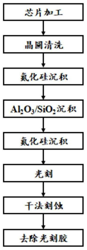
[0046] Taking the vertical cavity surface emitter as an example, silicon nitride-Al is deposited in the product process 2 o 3 / SiO 2 -Silicon nitride multilayer film is used as protective layer, and the relevant parameters of composition and structure of this protective film are as shown in table 1:

[0047] Table 1 Composition and structure of protective film

[0048] deposition sequence Film type membrane thickness Refractive index 1 Silicon nitride 50 2.0 2 al 2 o 3

50 1.65 3 SiO 2

30 1.46 4 Silicon nitride 190 2.0

[0049] The prepared protective film can achieve a light reflectance of less than 1% at a wavelength of 850nm, so as to reduce the reflectance of the cavity facing the light of this wavelength.

[0050] The performance of the same laser without a protective film structure and the laser with a protective film structure was tested. The results show that the optical anti-reflection effect of the laser...

Embodiment 2

[0052] The photodiode is used as a device that receives light and converts it into a current signal, and silicon nitride-Al is deposited in the product process 2 o 3 / SiO 2 / Al 2 o 3 / SiO 2 -Silicon nitride multilayer film is used as protective layer, and the relevant parameters of composition and structure of this protective film are as shown in table 2:

[0053] Table 2 Composition and structure of protective film

[0054] deposition sequence Film type membrane thickness Refractive index 1 Silicon nitride 30 2.0 2 al 2 o 3

50 1.65 3 SiO 2

30 1.46 4 al 2 o 3

50 1.65 5 SiO 2

30 1.46 6 Silicon nitride 40 2.0

[0055] The prepared protective film can achieve a light reflectance of less than 1% at a wavelength of 1550nm, which improves the light conversion efficiency of the photodiode, and the dark current, responsivity and frequency characteristics of the photodiode without the protectiv...


PUM

PropertyMeasurementUnit
thicknessaaaaaaaaaa
thicknessaaaaaaaaaa
thicknessaaaaaaaaaa

Abstract

The invention discloses a protective layer of a semiconductor photoelectric chip and a production process of a semiconductor. The protective layer of the photoelectric chip comprises a first silicon nitride layer, an Al2O3/SiO2 layer and a second silicon nitride layer from bottom to top in sequence, and a sandwich structure is presented. The process for producing the semiconductor device with the protective layer comprises the following steps of processing a chip; cleaning the wafer; depositing a first silicon nitride layer on the surface of the wafer; depositing an Al2O3/SiO2 layer on the first silicon nitride layer; depositing a second silicon nitride layer on the Al2O3/SiO2 layer; and producing the required semiconductor through a photoetching process, a dry etching process and photoresist removal. The protective layer with a sandwich structure fully utilizes the characteristics of different thin film layers to realize long-acting blocking of water vapor, improves the durability of the device, does not affect the electrical performance of the semiconductor device, can adjust the reflection property to light by adjusting the structure and film thickness of the protective layer, and is simple in production process, low in cost, and good in efficiency. Good application prospects are realized.

Description

technical field [0001] The invention relates to the technical field of semiconductors, in particular to a protective layer for a semiconductor optoelectronic chip and a preparation process for the semiconductor. Background technique [0002] Semiconductor optoelectronic chips include LEDs, lasers, photodiodes, etc., and their materials are compound semiconductors such as InP, GaAs, and GaN, which are easily oxidized when exposed to air. Water vapor has the effect of accelerating oxidation and erosion on the surface electrodes and materials of the semiconductor laser chip, and eventually causes the photoelectric chip to fail. In order to avoid this problem, the commonly used techniques are tube and shell encapsulation and application of sealing glue. Among them, the tube and shell packaging technology (the structure is as attached figure 1 As shown) is to mount the photoelectric chip on the base, and the TO tube cap is fixed to the base by welding or glue bonding. This meth...

Claims


Application Information

Patent Timeline
Patent Type & Authority Applications(China)
IPC IPC(8): H01L31/0216H01L31/18H01S5/028H01S5/183
CPCH01L31/02161H01L31/1868H01S5/183H01S5/0282Y02P70/50
Inventor 张登巍冯丽彬李鑫
Owner 苏州鼎芯光电科技有限公司
Why Eureka
Try Eureka